Method for preparing monodisperse copper sulfide semiconductor nano particles
A nanoparticle and copper sulfide technology, applied in the direction of copper sulfide, etc., can solve the problems of long reaction time, high production cost, easy product agglomeration, etc., and achieve the effect of uniform particle size, low cost and high yield
- Summary
- Abstract
- Description
- Claims
- Application Information
AI Technical Summary
Problems solved by technology
Method used
Image
Examples
Embodiment 1
[0019] Take 50ml 0.08M Cu(NO 3 ) 2 solution, add 0.08M Na under stirring 2 S solution 60ml, react for 10-30 minutes. Then add an ethanol solution of N,N-dibutyl potassium dithioformate, and continue to stir and react for 4-8 hours. After the reaction, the product was centrifuged, and the obtained solid was rinsed with a large amount of ethanol-water mixed solution, and then dried in vacuum at 80° C., and the obtained black solid was copper sulfide semiconductor nanoparticles.
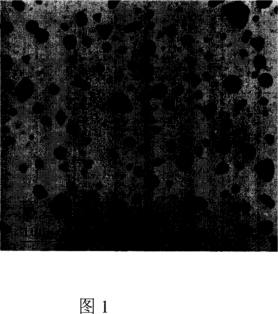
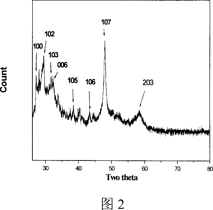
[0020] Figure 1 is a transmission electron micrograph of the prepared copper sulfide semiconductor nanoparticles, it can be seen that the prepared nanoparticles have a uniform particle size, no agglomeration, and an average particle size of 30nm. Figure 2 is the XRD pattern of the prepared nanoparticles, from which it can be seen that the prepared nanocomposite contains copper sulfide.
Embodiment 2
[0022] Take 2.0×10 -3 mol of CTAB dissolved in 50ml of 0.08M Cu(NO 3 ) 2 solution, add 0.08M Na under stirring 2 S solution 60ml, react for 10-30 minutes. Then add the ethanol solution of N,N-dioctyl potassium dithioformate, and continue stirring for 4-8 hours. After the reaction, the product was centrifuged, and the obtained solid was rinsed with a large amount of ethanol-water mixed solution, and then dried in vacuum at 80° C., and the obtained black solid was copper sulfide semiconductor nanoparticles.
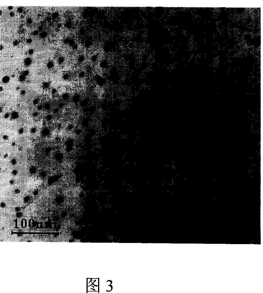
[0023] FIG. 3 is a transmission electron micrograph of the prepared copper sulfide semiconductor nanoparticles. It can be seen that the prepared nanoparticles have a uniform particle size, no agglomeration, and an average particle size of 10 nm.
Embodiment 3
[0025] Take 4.0×10 -3 mol of CTAB dissolved in 50ml of 0.08M Cu(NO 3 ) 2 solution, add 0.08M Na under stirring 2 S solution 60ml, react for 10-30 minutes. Then add the ethanol solution of N,N-dibutyl sodium dithioformate, and continue to stir the reaction for 4-8 hours. After the reaction, the product was centrifuged, and the obtained solid was rinsed with a large amount of ethanol-water mixed solution, and then dried in vacuum at 80° C., and the obtained black solid was copper sulfide semiconductor nanoparticles.
[0026] FIG. 4 is a transmission electron micrograph of the prepared copper sulfide semiconductor nanoparticles. It can be seen that the prepared nanoparticles have a uniform particle size, no agglomeration, and an average particle size of 4nm.
PUM
| Property | Measurement | Unit |
|---|---|---|
| particle size | aaaaa | aaaaa |
| particle size | aaaaa | aaaaa |
| particle size | aaaaa | aaaaa |
Abstract
Description
Claims
Application Information
 - Generate Ideas
- Intellectual Property
- Life Sciences
- Materials
- Tech Scout
- Unparalleled Data Quality
- Higher Quality Content
- 60% Fewer Hallucinations
Browse by: Latest US Patents, China's latest patents, Technical Efficacy Thesaurus, Application Domain, Technology Topic, Popular Technical Reports.
© 2025 PatSnap. All rights reserved.Legal|Privacy policy|Modern Slavery Act Transparency Statement|Sitemap|About US| Contact US: help@patsnap.com


