
Electrostatic chuck

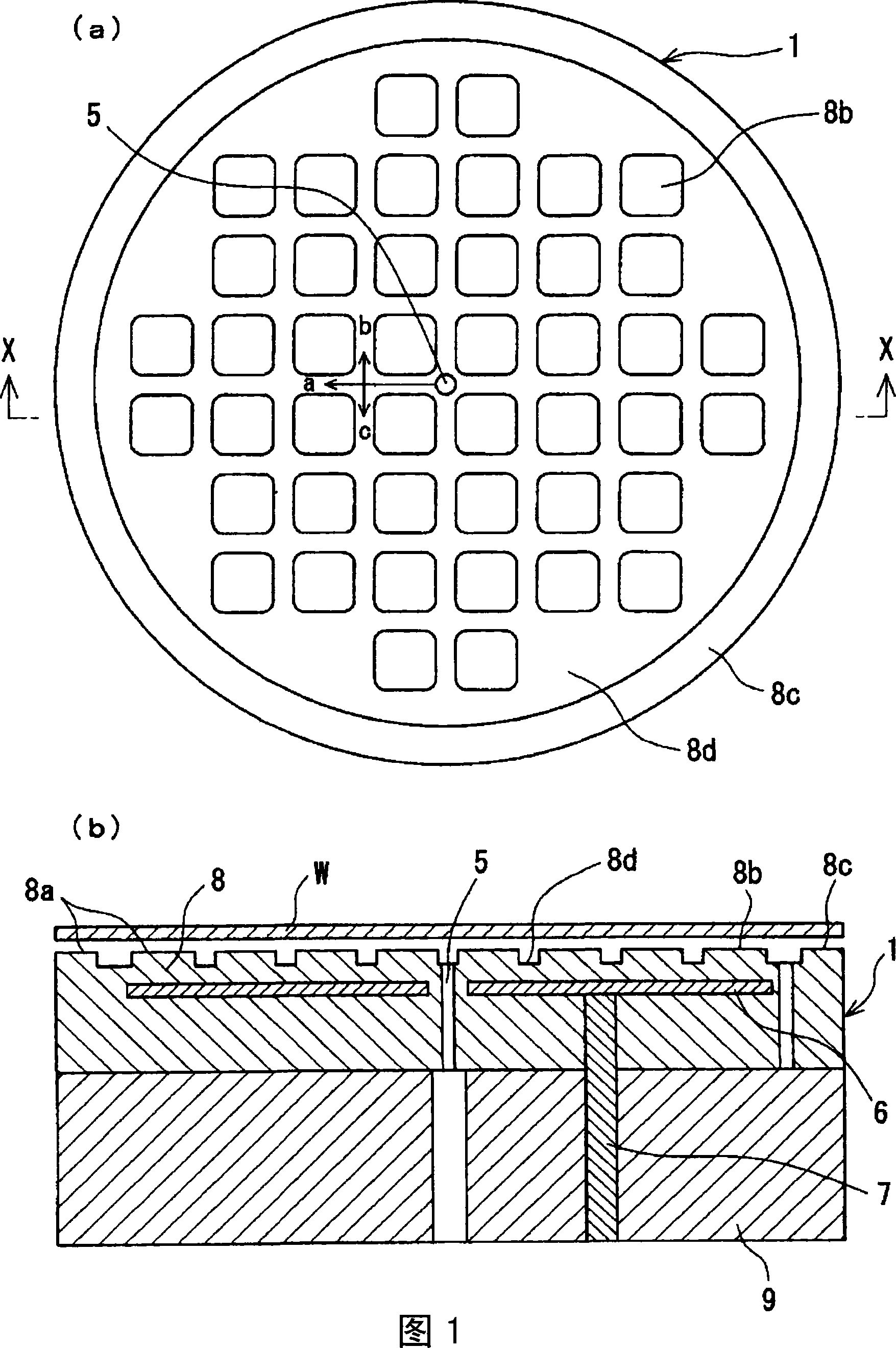
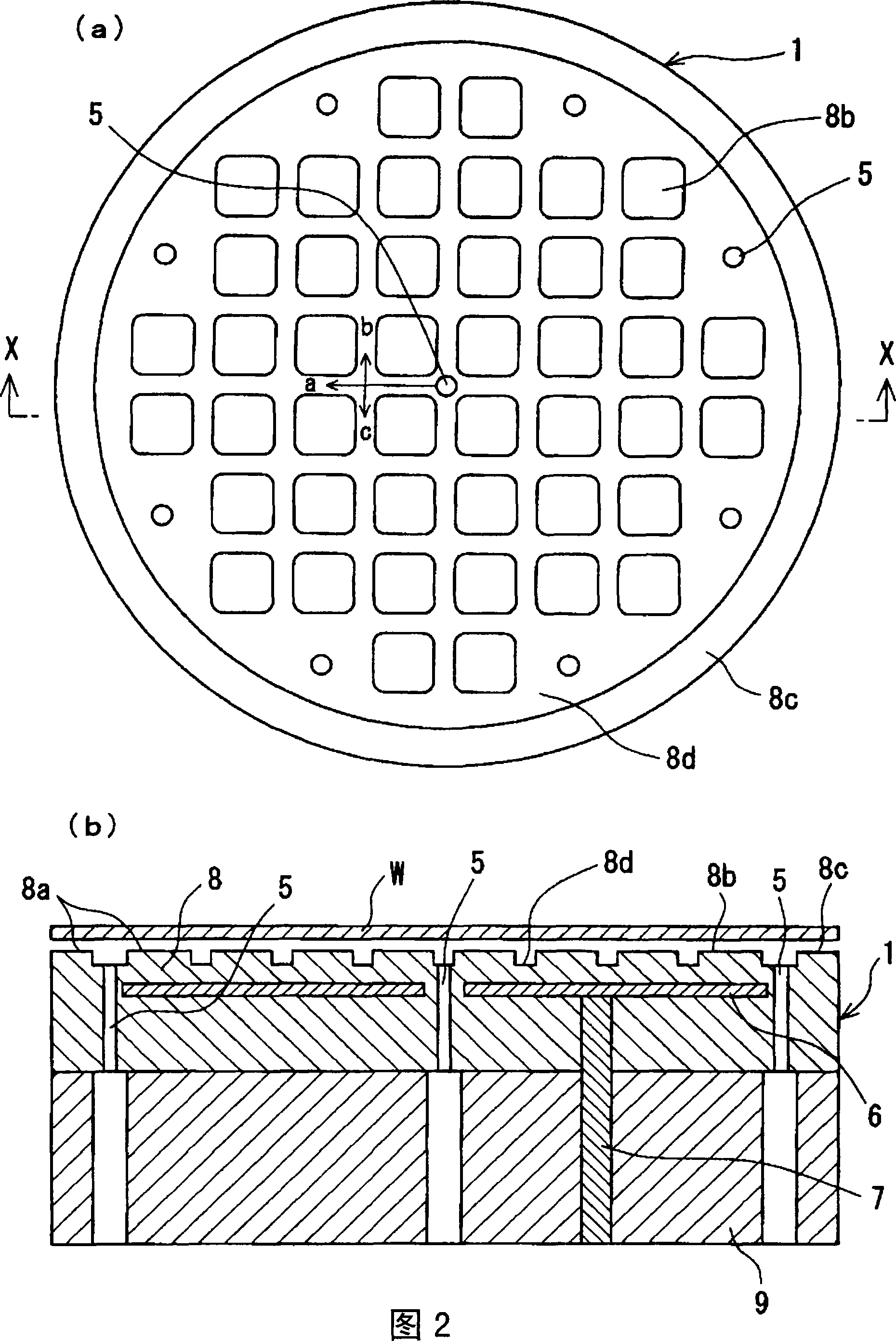
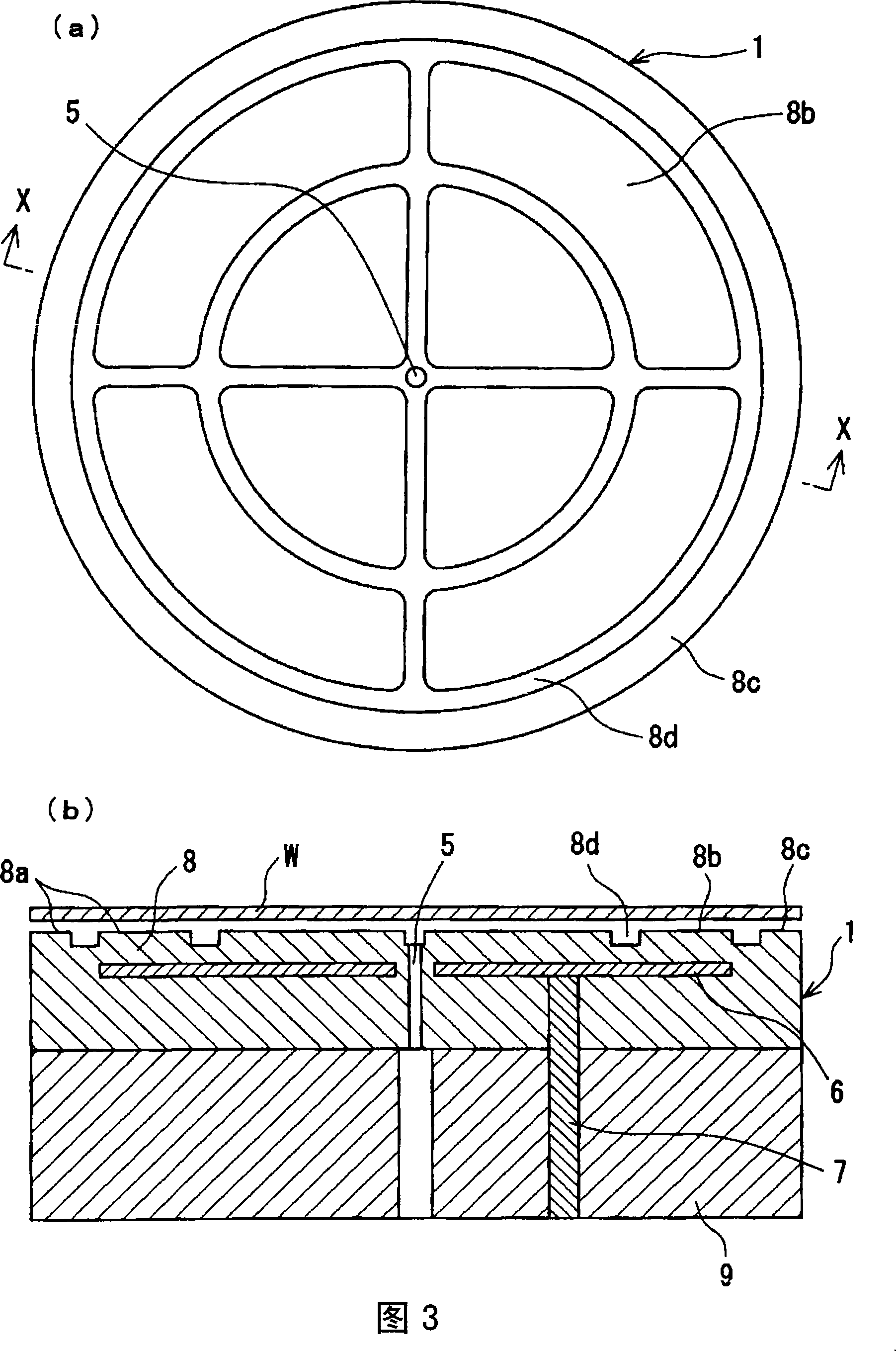
一种静电卡盘、电极的技术,应用在电路、电气元件、应用静电吸引力的保持装置等方向,能够解决电介质层绝缘破坏等问题,达到提高均热性、缩短饱和温度的时间的效果

Inactive Publication Date: 2007-08-01
KYOCERA CORP
View PDF4 Cites 19 Cited by
  • Summary
  • Abstract
  • Description
  • Claims
  • Application Information

AI Technical Summary

Problems solved by technology

In order to increase the adsorption force without narrowing the gas flow path, it is necessary to apply a high voltage to the electrode embedded in the electrostatic chuck. However, if the cycle of applying the high voltage and releasing the high voltage is repeated, the dielectric of the electrostatic chuck will be damaged. The problem of layer insulation breakdown

Method used


Image

  • Electrostatic chuck
  • Electrostatic chuck
  • Electrostatic chuck

Examples


Embodiment 1

[0097] Specific examples of the present invention will be described below using an electrostatic chuck as an example.

[0098] First of all, the aluminum oxide Al 2 o 3 The formed plate-shaped body will be described as an example. Al with a purity of 99.9% by mass at an average particle size of 1.0 μm 2 o 3 0.2% by mass of CaO and SiO2 are added to the powder as a sintering aid, and a binder and a solvent are added to make a slurry, which is then formed into multiple green sheets of alumina by the doctor blade method.

[0099]On one of the alumina green sheets, a metal paste of molybdenum, which is an electrode for adsorption, was printed in a predetermined electrode pattern by a screen printing method. Further, the remaining alumina green sheets were laminated on the surface opposite to the surface on which the metal paste was applied. On the other hand, a plurality of alumina green sheets on which the metal paste was not printed were stacked, and power feeding holes wit...

Embodiment 2

[0117] An electrostatic chuck was produced in the same manner as in Example 1. The groove is machined by a Machining Center, so that the dimensions of the R shape connecting the groove and the curved surface of the convex part are 0.005, 0.01, 0.05, and 0.1mm, respectively, and the dimensions of the R shape connecting each side of the convex part are 0.5mm. Accordingly, an electrostatic chuck was fabricated in the same manner as No. 3 of Example 1. However, in making the dimension of the R-shape connecting the groove and the curved surface of the convex part 0.1 mm, the depth of the groove was made 0.1 mm. This was evaluated in the same manner as in Example 1. The results are shown in Table 2.

[0118] (Table 2)

[0119] Sample No.

Dimensions of R shape (mm)

Wafer temperature distribution (°C)

up to the saturation temperature

time (seconds)

7

0.005

0.8

2.4

8

0.01

0.7

2.2

9

0.05

0.6

2.2...

Embodiment 3

[0123] An electrostatic chuck was produced in the same manner as in Example 1. Make the R of the corner of the convex portion 2 be 0.5mm, and change the abrasive grains of sandblasting, make the arithmetic mean roughness Ra of the groove 4 be 0.3, 0.5, 1.0, 2.0, 2.5, and others are the same as in Example 1 Make an electrostatic chuck. And it evaluated similarly to Example 1. The results are shown in Table 2.

[0124] (table 3)

[0125] Sample No.

Arithmetic mean of groove

Roughness Ra(μm)

Wafer temperature distribution

(℃)

up to saturation temperature

time (seconds)

12

0.3

0.4

2.0

13

0.5

0.5

2.1

14

1.0

0.6

2.3

15

2.0

0.7

2.4

16

2.5

1.2

3.2

[0126] The temperature distribution of the wafers of sample Nos. 12 to 15 in which the arithmetic mean roughness Ra of the bottom surfa...


PUM


Abstract

A purpose of the present invention is to provide an electrostatic chuck which has such a high uniformity of heat that the time for arriving at a saturated temperature is short, and which has a high resistance property against the cycle of a voltage. To achieve above-mentioned purpose, there is provided an electrostatic chuck comprising a plate-shaped body which has a pair of main surfaces, on one of which a wafer is placed, and electrodes for adsorbing the wafer, which are provided on the other surface of the plate-shaped body or in the plate-shaped body, characterized in that it comprises at least one through-hole for guiding gases, which is formed in the plate-shaped body, gas tunnels which are formed by several convex parts and are formed so as to be communicated with the through-hole, wherein the shape of the convex part is shaped to have 4 sides and 4 arc-shaped parts for connecting the 4 sides and wherein the convex parts are regularly provided on the surface for placing a wafer.

Description

technical field [0001] The invention relates to an electrostatic chuck for electrostatically adsorbing a semiconductor wafer in a semiconductor manufacturing process, or for absorbing a liquid crystal substrate in a flat-panel display manufacturing process. Background technique [0002] Conventionally, in semiconductor manufacturing processes, electrostatic chucks that hold wafers by electrostatic attraction are used in etching processes for microfabrication of semiconductor wafers (hereinafter referred to as wafers) or film formation processes for forming thin films. [0003] The electrostatic chuck uses the upper surface of the dielectric layer as a mounting surface on which the wafer as the object to be adsorbed is placed, and has electrodes for electrostatic adsorption on the lower surface of the dielectric layer. By applying a voltage between the wafer and the electrode for electrostatic attraction, an electrostatic attraction force is generated, whereby the wafer is fi...

Claims


Application Information

Patent Timeline
Patent Type & Authority Applications(China)
IPC IPC(8): H01L21/68H02N13/00
CPCH01L21/6831H02N13/00H01L21/687
Inventor 神谷哲横山清
Owner KYOCERA CORP
Learn More