
Two-dimensional ultrasound transducer arrays

A technology of ultrasonic transducers and arrays, applied in the field of transducer arrays

Inactive Publication Date: 2007-07-25
KONINKLIJKE PHILIPS ELECTRONICS NV
View PDF1 Cites 16 Cited by
  • Summary
  • Abstract
  • Description
  • Claims
  • Application Information

AI Technical Summary

Problems solved by technology

However, all known bumping technologies cannot consistently produce bumps with an aspect ratio of footprint (width) to height greater than 1

Method used


Image

  • Two-dimensional ultrasound transducer arrays
  • Two-dimensional ultrasound transducer arrays
  • Two-dimensional ultrasound transducer arrays

Examples


Embodiment Construction

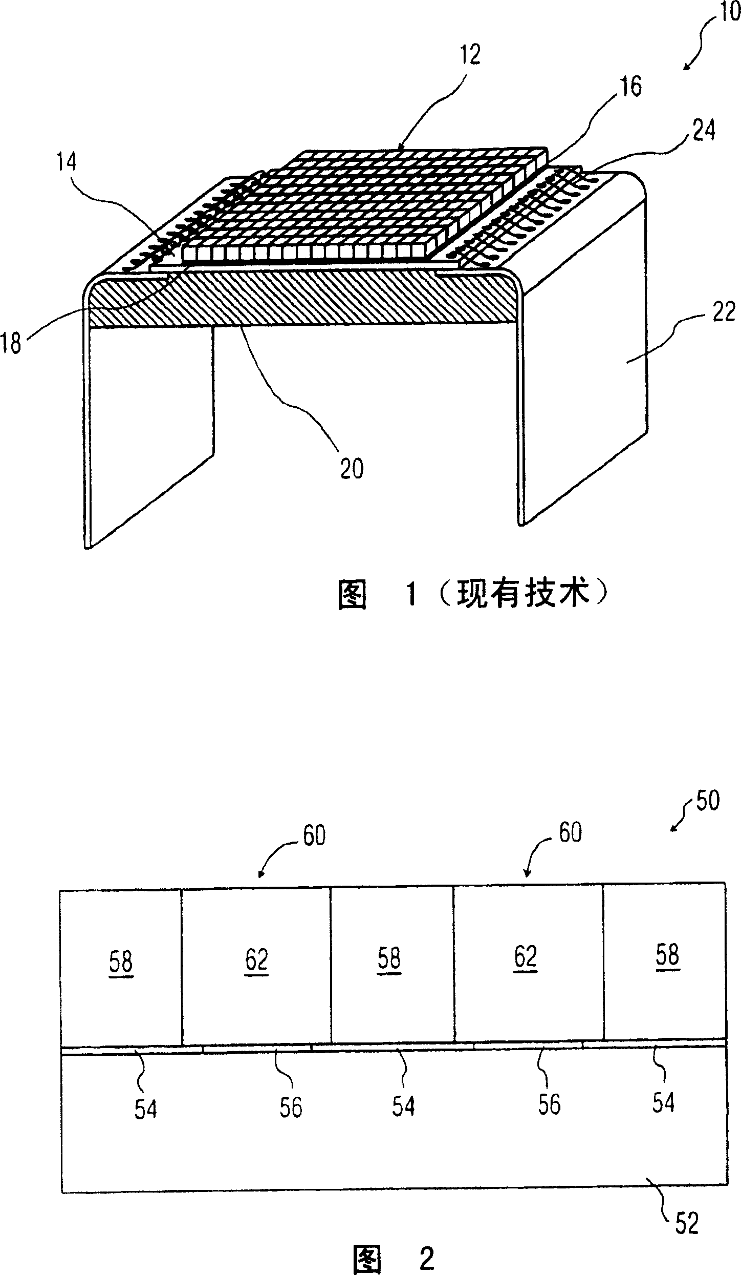
[0019] In integrated circuit fabrication, a semiconductor wafer typically contains multiple integrated circuit dies that have not been separated into individual devices. Each integrated circuit die typically contains circuitry for performing desired functions as required by a particular integrated circuit application. For example, integrated circuit applications may include ultrasound transducer applications. Additionally, ultrasound transducer applications may include cardiac applications, abdominal applications, transesophageal (TEE) applications, or other diagnostic or therapeutic ultrasound applications.

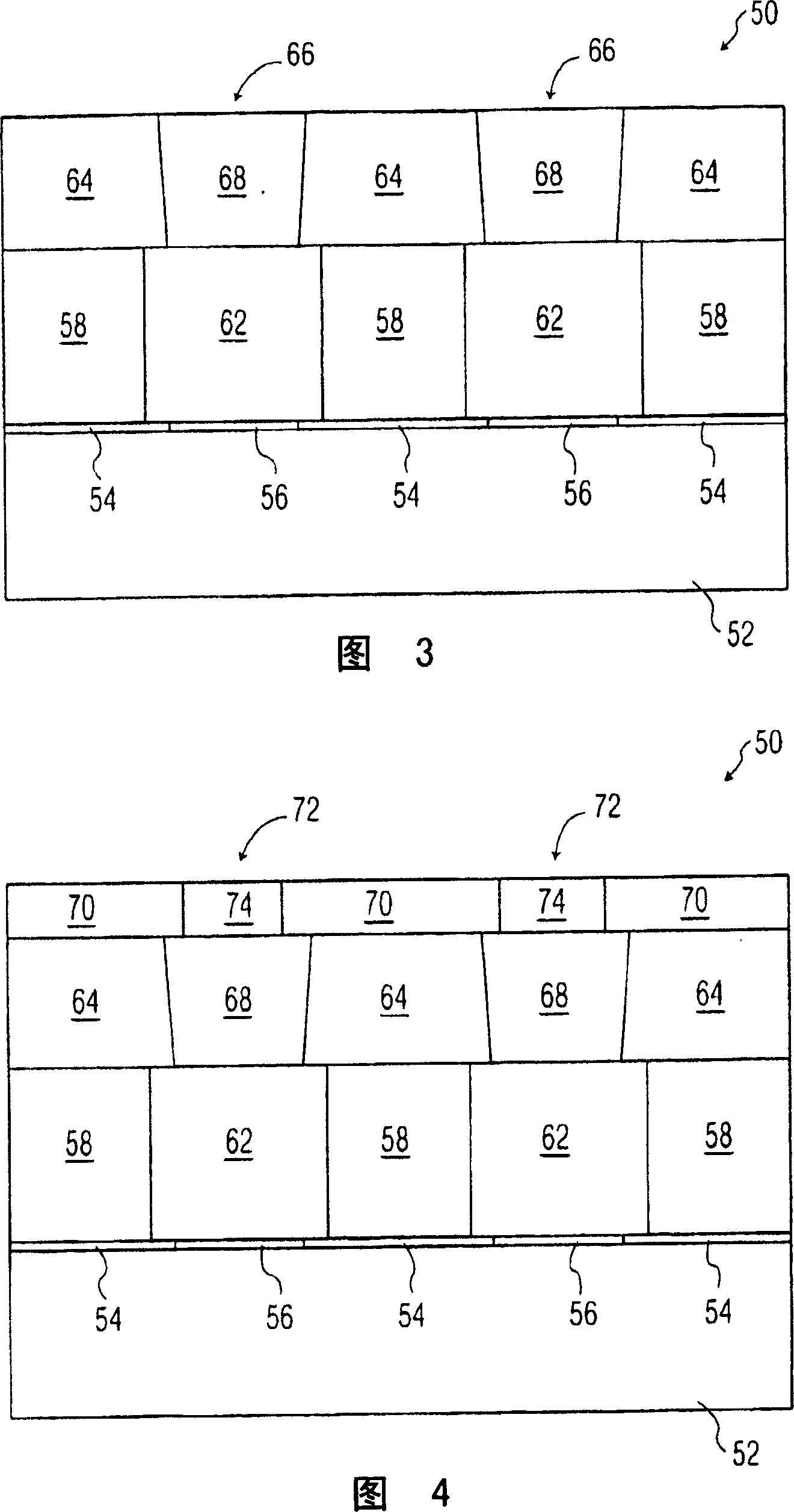
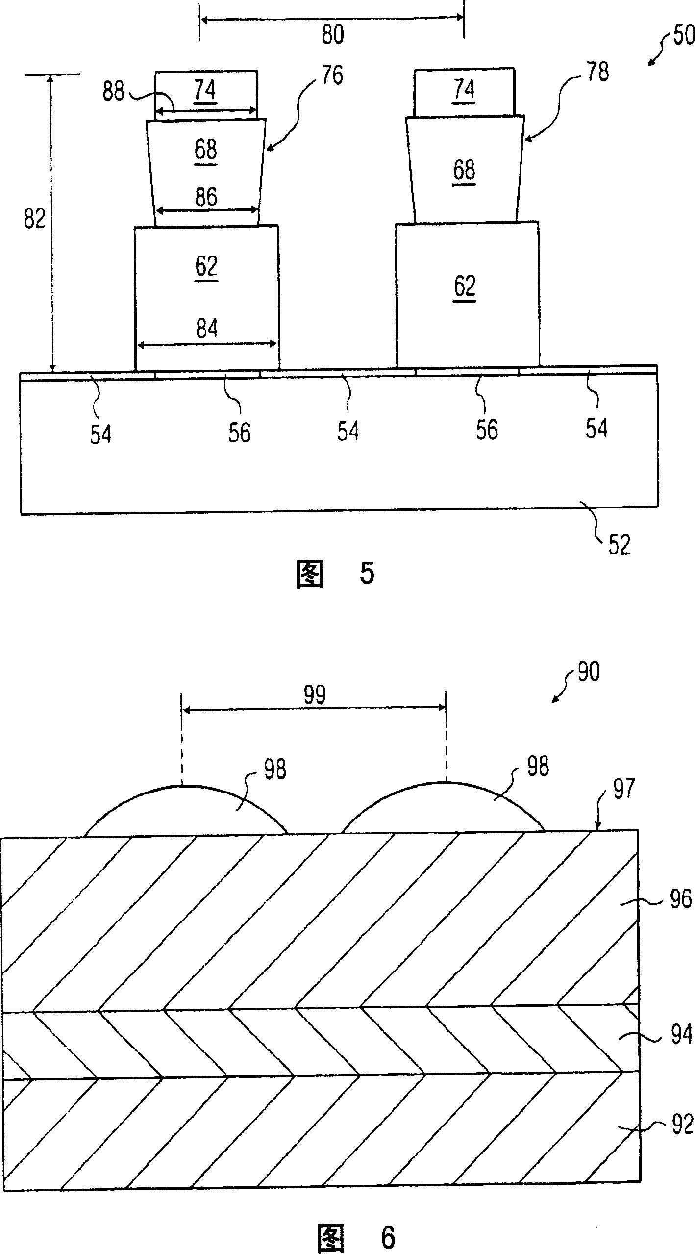
[0020] For ultrasound devices, a simplified ultrasound transducer construction procedure may include the following steps. For example, the process begins by obtaining a wafer containing a desired ultrasound transducer IC, eg, from an Application Specific Integrated Circuit (ASIC) vendor. A wafer bumping process according to one embodiment of the present invention is pe...


PUM

PropertyMeasurementUnit
Pitchaaaaaaaaaa
Thicknessaaaaaaaaaa

Abstract

An ultrasound transducer (100) comprises an integrated circuit (52) and an array of acoustic elements (92,94,96) coupled to the integrated circuit via flip chip bumps (76,78). The flip chip bumps comprise high aspect ratio bumps having an aspect ratio greater than 1:1. The aspect ratio comprises a ratio of a bump height (82) to a bump width (84).

Description

[0001] This application is related to the patent application entitled "Transducer Arrays for Medical Ultrasound and Method of Making the Same" by Bernard Savord et al. of Attorney Docket US040334 filed at the same time as this case, which is hereby incorporated by reference in its entirety. technical field [0002] The present invention relates generally to transducer arrays for medical ultrasound, and more particularly to methods and apparatus for implementing high aspect ratio bumps for flip-chip two-dimensional arrays. Background technique [0003] In medical ultrasound, two-dimensional transducer arrays are commonly used to transmit and receive ultrasound or acoustic waves during ultrasonic diagnostic imaging. Prior art two-dimensional arrays typically comprise planar arrays with approximately three thousand (3,000) transducer elements. In one type of ultrasound transducer design, all transducer elements of the array are attached and individually electrically connected t...

Claims


Application Information

Patent Timeline
IPC IPC(8): G01S15/89G01S7/521B06B1/06G10K11/00A61B8/14
CPCH01L2224/83851H01L2924/01082G01S7/52079H01L2924/0781H01L2924/01049H01L2224/81903H01L2224/13144G01S15/8925H01L2924/01029H01L2924/00013H01L2224/1147H01L2224/83102H01L2224/13083H01L2224/13016H01L24/11H01L2924/014H01L2924/01013H01L2224/11902H01L2924/0665G01S7/5208H01L2224/2919H01L2224/92125H01L24/13H01L2924/1433H01L2924/01079H01L2224/1308H01L2224/838H01L2924/14H01L24/83H01L24/29H01L2924/01033H01L2924/01078B06B1/0629H01L2924/00014H01L2924/00011Y10T29/42H01L2224/13099H01L2924/00H01L2224/0401
Inventor W·苏多尔
Owner KONINKLIJKE PHILIPS ELECTRONICS NV
Learn More