Metal trench de-noise structure and method for forming the same

a trench denoise and trench technology, applied in the direction of diodes, semiconductor devices, electrical devices, etc., can solve the problems of intensifying noise interference, purifying digital signal itself or its associated noise being likely to become the noise of other types of more sensitive signal types, etc., to reduce coupling noise interference, reduce noise, and reduce noise. the effect of interferen

Active Publication Date: 2018-05-22
REALTEK SEMICON CORP
View PDF49 Cites 0 Cited by
  • Summary
  • Abstract
  • Description
  • Claims
  • Application Information

AI Technical Summary

Benefits of technology

[0008]In view of this, the present invention therefore proposes a metal trench de-noise structure which is used to suppress the interference of coupling noise in the substrate. The metal trench de-noise structure of the present invention has floating or grounded metal piles deeply rooted in the substrate, to quickly shield or drain an interference of coupling noise in the substrate, for example noise from a digital region, so that a signal in a more sensitive region, such as a signal from an analog region, are less easily coupled or interfered.
[0009]The present invention in a first aspect proposes a metal trench de-noise structure. The metal trench de-noise structure of the present invention includes a substrate, a trench, an insulating layer, an inter-layer dielectric layer, and a metal layer. The trench is disposed in the substrate. The insulating layer is disposed on the sidewall of the trench. The inter-layer dielectric layer covers the substrate and the insulating layer. The metal layer is disposed on the substrate and penetrates the inter-layer dielectric layer to fill up the trench. The metal layer is either grounded or floating to quickly suck the coupling noise in the substrate, or further to shield noise from other regions, to avoid the coupling hetero signals in the substrate interfering with signals from other regions.

Problems solved by technology

On the other hand, either a pure digital signal itself or its associated noise is likely to become the noise of other kinds of more sensitive signal types.
In other words, the digital signal itself is indifferent to noise, but it could be the source of noise to other types of signals which are more sensitive to noise.
Considering the increasing element density on chips and different element regions are getting closer and closer to each other, they intensify the interference of noise.

Method used


Image

  • Metal trench de-noise structure and method for forming the same
  • Metal trench de-noise structure and method for forming the same
  • Metal trench de-noise structure and method for forming the same

Examples


Embodiment Construction

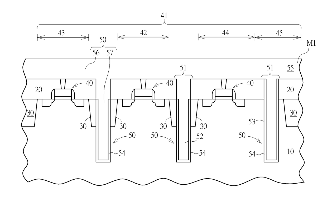
[0018]The present invention provides a metal trench de-noise structure and a method for forming the metal trench de-noise structure. The metal layer in the metal trench de-noise structure goes deeply in the substrate to form floating or grounded metal piles. Such metal piles are able to shield or to quickly suck the interference of coupling noise in the substrate. This ensures the purity and cleanness of individual signals.

[0019]First, the present invention provides a method of forming a metal trench de-noise structure. FIG. 1 to FIG. 7 illustrates the method for forming a metal trench de-noise structure of the present invention. First, as shown in FIG. 1, a substrate 10 is provided. The substrate 10 may be a semiconductor substrate, for example a silicon substrate, an epitaxial silicon substrate, a silicon germanium substrate, a silicon carbide substrate or a silicon-on-insulator (SOI) substrate, but it is not limited to this. The substrate 10 is usually grounded. In addition, in t...


PUM

PropertyMeasurementUnit
depthaaaaaaaaaa
frequencyaaaaaaaaaa
frequenciesaaaaaaaaaa

Abstract

A metal trench de-noise structure includes a trench disposed in a substrate, an insulating layer deposited on the sidewall of the trench, an Inter-Layer Dielectric layer covering the substrate and the insulating layer, and a metal layer penetrating the Inter-Layer Dielectric layer to fill up the trench. The metal layer may be grounded or floating.

Description

CROSS REFERENCE TO RELATED APPLICATION[0001]This application claims the benefit of Taiwanese Application 102131716, filed Sep. 3, 2013.BACKGROUND OF THE INVENTION[0002]1. Field of the Invention[0003]The present invention generally relates to a metal trench de-noise structure. In particular, the present invention is directed to a deep metal trench de-noise structure, to avoid sensitive signal region interfering with coupling noise in the substrate.[0004]2. Description of the Prior Art[0005]Generally speaking, as shown in FIG. 11, semiconductor elements are usually various semiconductor elements 40 disposed on the element region 41 of the substrate 10. Optionally, the element region 41 may include various electronic elements. For example, various adjacent element regions 41 include electronic elements generating different types of signals. For instance, various adjacent element regions 41 may be a digital circuit element region 42, a radio frequency (RF) circuit element region 43, or ...

Claims


Application Information

Patent Timeline
Patent Type & Authority Patents(United States)
IPC IPC(8): H01L21/768H01L21/74H01L29/94H01L27/06H01L29/66
CPCH01L21/76807H01L21/743H01L21/76898H01L29/66181H01L29/945H01L27/0629H01L2223/6616H01L21/765
Inventor YEH, TA-HSUN
Owner REALTEK SEMICON CORP
Why Eureka
Try Eureka