
Multilayer ceramic capacitor

a ceramic capacitor and multi-layer technology, applied in the direction of fixed capacitor details, fixed capacitors, printed circuit non-printed electric components association, etc., can solve the problems of peeling between the capacitors and reduce the reliability of the component, and achieve the effect of reliable resistance to moistur

Active Publication Date: 2018-01-30
MURATA MFG CO LTD
View PDF11 Cites 1 Cited by
  • Summary
  • Abstract
  • Description
  • Claims
  • Application Information

AI Technical Summary

Benefits of technology

The design achieves robust adhesion between the capacitor and the resin, preventing peeling and ensuring reliable moisture resistance, even under external forces.

Problems solved by technology

Such capacitors as in Japanese Patent Application Laid-Open No. 2002-203735 cause the problem of peeling between the capacitors and interlayer resin insulating layers or adhesives in the multilayer printed wiring boards in contact with the capacitors, when the capacitors are built into multilayer printed wiring boards.
Therefore, peeling between the multilayer ceramic capacitors and the resin in the multilayer printed wiring boards has the possibility of causing problems such as decreased component reliability due to ingress of moisture from the peeled sites, and fractured portions connected to via (small-diameter hole for the passage of signals) electrodes formed in the multilayer printed wiring boards.

Method used


Image

  • Multilayer ceramic capacitor
  • Multilayer ceramic capacitor
  • Multilayer ceramic capacitor

Examples


experimental examples

[0157]In experimental examples, respective samples of multilayer ceramic capacitors were prepared according to the following examples and comparative examples.

1. Preparation of Sample for Evaluation

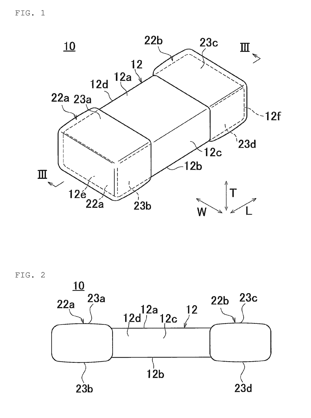
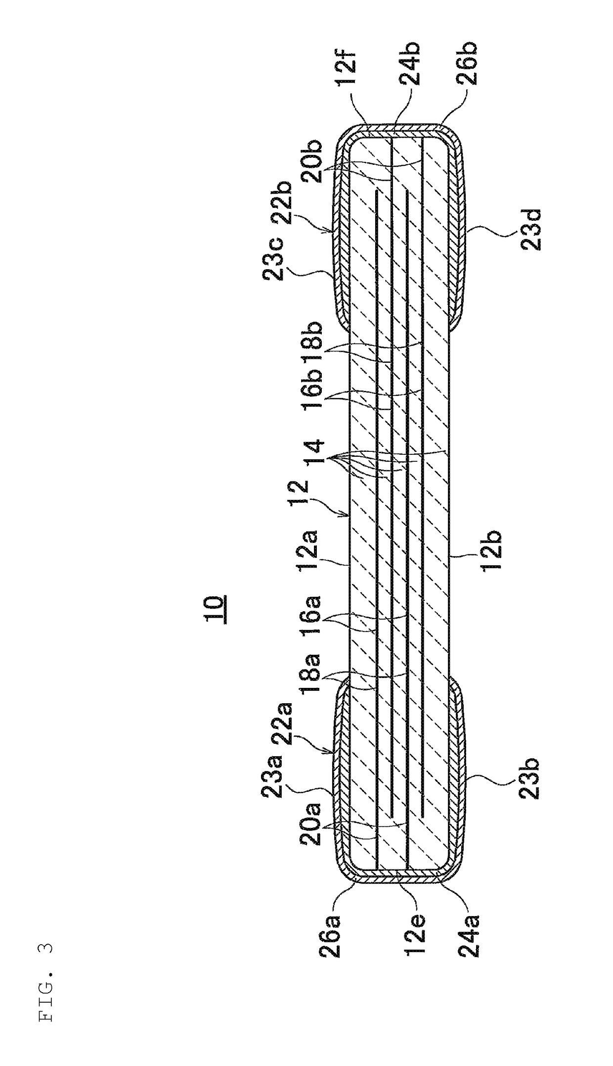
[0158]In the experimental examples, samples for the evaluation of the multilayer ceramic capacitor 10 were prepared by controlling the arithmetic mean roughness (Ra) at the surfaces of the external electrodes 22a, 22b, without control for impurity reduction in the step S8 of the manufacturing method mentioned in the previously described preferred embodiment, and control for changing the position of the maximum thickness of the base paste formed on the principal surfaces 12a, 12b of the ceramic body 12 in the step S5 thereof. The target dimensions of the multilayer ceramic capacitor 10 are about 1.0 mm in dimension in the length direction L, about 0.5 mm in dimension in the width direction W, and about 0.15 mm in dimension in the height direction T.

[0159]Respective samples according to Exa...


PUM

PropertyMeasurementUnit
heightaaaaaaaaaa
widthaaaaaaaaaa
widthaaaaaaaaaa

Abstract

A multilayer ceramic capacitor provided in a multilayer printed wiring board includes a ceramic body with a plurality of ceramic layers and internal electrodes stacked, and an external electrode including a base layer that includes a sintered metal containing a metal and glass and a plated layer provided on the surface of the base layer, which is provided on an end surface of the ceramic body to be connected to the internal electrodes. The external electrode includes a principal surface portion disposed on a principal surface of the ceramic body. The outermost layer of the plated layer includes a Cu plated layer. The ratio of arithmetic mean roughness (Ra) at the surface of the ceramic body / arithmetic mean roughness (Ra) at the surface of the external electrode satisfies a condition: about 0.06≦the arithmetic mean roughness (Ra) at the surface of the ceramic body / the arithmetic mean roughness (Ra) at the surface of the external electrode≦about 0.97.

Description

BACKGROUND OF THE INVENTION[0001]1. Field of the Invention[0002]The present invention relates to a multilayer ceramic capacitor.[0003]2. Description of the Related Art[0004]In recent years, with the reduction in size and height for electronic devices such as cellular phones and portable music players, multilayer printed wiring boards mounted on the electronic devices have been progressively reduced in size. Accordingly, multilayer ceramic capacitors mounted on the multilayer printed wiring boards have been also progressively reduced in size and height.[0005]Some of the multilayer ceramic capacitors are built into multilayer printed wiring boards, such as the multilayer ceramic capacitor described in, for example, Japanese Patent Application Laid-Open No. 2002-203735. Because the multilayer ceramic capacitor in Japanese Patent Application Laid-Open No. 2002-203735 is built into a multilayer printed wiring board, there is a need for tight adhesion between the multilayer ceramic capaci...

Claims


Application Information

Patent Timeline
Patent Type & Authority Patents(United States)
IPC IPC(8): H01G4/30H01G4/232H05K1/11H01G4/012H05K1/18H01G4/12
CPCH01G4/2325H05K1/115H05K1/185H01G4/232H01G4/12H01G4/012H05K2201/10015H01G4/30
Inventor SASABAYASHI, TAKEHISA
Owner MURATA MFG CO LTD
Learn More