Wafer processing method

a processing method and wafer technology, applied in the direction of active medium materials, manufacturing tools, semiconductor/solid-state device testing/measurement, etc., can solve the problem that the workpiece cannot be processed at the desired position, and achieve the effect of high accuracy

Active Publication Date: 2018-01-16
DISCO CORP
View PDF3 Cites 5 Cited by
  • Summary
  • Abstract
  • Description
  • Claims
  • Application Information

AI Technical Summary

Benefits of technology

[0006]It is therefore an object of the present invention to provide a wafer processing method which can process a wafer at a desired position by using a laser beam even when there is an error in processing position due to any factor relating a laser processing apparatus.
[0010]Further, there is a possibility that the size and brightness of the beam plasma at the positions where the metal patterns are formed are different from those at the positions where the metal patterns are not formed, causing erroneous recognition of the laser processed groove. According to the present invention, in the case that the metal patterns for testing are formed on the division lines of the wafer at given intervals, the intervals and positions of the metal patterns are previously stored in the storage means, and kerf check is performed so as to avoid the metal patterns. Accordingly, the kerf check can be performed without erroneous recognition, so that the wafer can be processed with high accuracy.

Problems solved by technology

However, there is a problem such that the focused point of the laser beam cannot be set at a preset processing position due to any factor relating to a laser processing apparatus, such as strain generated in an optical system for the laser beam, so that the workpiece cannot be processed at a desired position.

Method used


Image

  • Wafer processing method
  • Wafer processing method
  • Wafer processing method

Examples


Embodiment Construction

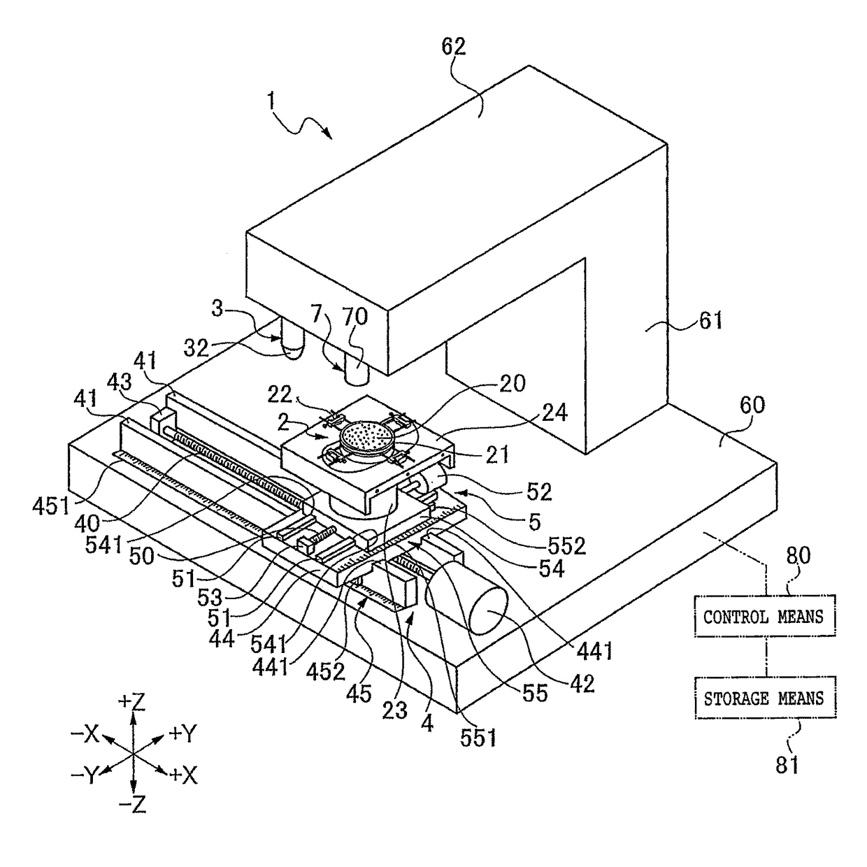
[0023]Referring to FIG. 1, there is depicted a laser processing apparatus 1 for use in performing a preferred embodiment of the present invention. The laser processing apparatus 1 is an apparatus for applying a pulsed laser beam to a wafer held on a chuck table 2 by using laser beam applying means 3, thereby laser-processing the wafer. The chuck table 2 is movable in the X direction (+X or −X direction) by operating X moving means 4 and also movable in the Y direction (+Y or −Y direction) by operating Y moving means 5.

[0024]The chuck table 2 includes a suction holding portion 20 for holding the wafer under suction, a frame 21 for supporting the suction holding portion 20 so as to surround the same, and a clamp portion 22 fixed to the outer circumference of the frame 21. The lower portion of the chuck table 2 is connected to a rotational drive portion 23 for rotating the chuck table 2. The rotational drive portion 23 is provided with an upper cover 24.

[0025]The X moving means 4 is pr...


PUM

PropertyMeasurementUnit
absorption wavelengthaaaaaaaaaa
repetition frequencyaaaaaaaaaa
timeaaaaaaaaaa

Abstract

Disclosed herein is a wafer processing method including a processed position measuring step of imaging an area including a beam plasma generated by applying a pulsed laser beam to a wafer, by using an imaging unit during the formation of a laser processed groove on the wafer, and next measuring the positional relation between the position of the beam plasma and a preset processing position. Accordingly, it is possible to check whether or not the laser processed groove is formed at a desired position, in real time during laser processing. If the position of the laser processed groove is deviated, the processed position can be immediately corrected.

Description

BACKGROUND OF THE INVENTION[0001]Field of the Invention[0002]The present invention relates to a wafer processing method for processing a wafer as measuring the positional relation between a preset processing position and an actually processed position by laser processing of the wafer.[0003]Description of the Related Art[0004]In a semiconductor device fabrication process, a plurality of electronic circuits such as integrated circuits (ICs) and large-scale integrations (LSIs) are formed on the front side of a substantially disk-shaped workpiece such as a semiconductor wafer. The back side of the workpiece thus having the plural electronic circuits is ground to reduce the thickness of the workpiece to a predetermined thickness. Thereafter, a device area of the workpiece where the electronic circuits are formed is cut along division lines called streets by applying a laser beam to thereby divide the workpiece into a plurality of device chips (see Japanese Patent Laid-Open No. 2012-15122...

Claims


Application Information

Patent Timeline
Patent Type & Authority Patents(United States)
IPC IPC(8): H01L21/268H01S3/16H01L21/66H01L23/544H01S3/11H01L21/687H01L21/683H01L21/68H01L21/67
CPCH01L22/20H01L21/268H01L21/67282H01L21/681H01L21/6838H01L22/32H01L23/544H01S3/11H01S3/163H01L21/68764H01L2223/5446B23K26/364B23K26/705B23K26/402H01L21/78H01L21/67092H01L21/67259H01L2223/5442H01L2223/54426H01L2223/54453H01L21/76H01L21/67242H01L22/12H01L21/68
Inventor IWAMOTO, TAKUOHKUBO, HIRONARIKUKI, JUNICHIODANAKA, KENTARO
Owner DISCO CORP
Why Eureka
Try Eureka