Metal-oxide semiconductor (MOS) transistor offset-cancelling (OC), zero-sensing (ZS) dead zone, current-latched sense amplifiers (SAs) (CLSAs) (OCZS-SAs) for sensing differential voltages

a metal-oxide semiconductor and transistor technology, applied in the field of sensing circuitry, can solve the problem that the oczs-sa consumes even less layout area, and achieve the effect of less layout area

Active Publication Date: 2017-12-26
QUALCOMM TECHNOLOGIES INC +1
View PDF11 Cites 19 Cited by
  • Summary
  • Abstract
  • Description
  • Claims
  • Application Information

AI Technical Summary

Benefits of technology

[0010]In further exemplary aspects disclosed herein, to avoid the need to provide both sensing capacitor circuits to store the data and reference input voltages during an input phase, and then separate sense amplifier capacitors to store the data and reference input voltages at the gates of the input and complement input transistors during a voltage capture phase, an OCZS-SA is configured to pre-charge the gates of the input and complement input transistors to a supply node before the data and reference input voltages are received in voltage captures phases. Then, in a discharge phase before the voltage capture phases, the gates of the input and complement input transistors are discharged from the supply node to the threshold voltages of their respective input and complement input transistors to cancel their offset voltages while the data and reference input voltages are received and stored in sense amplifier capacitors coupled to the respective gates of the input and complement input transistors. In this manner, additional layout area that would otherwise be consumed with additional sensing capacitor circuits is avoided. Further, the sense amplifier capacitors in the OCZS-SA for storing the data and reference input voltages can be smaller, thus causing the OCZS-SA to consume even less layout area, because the OCZS-SA can still achieve the desired offset variation voltage.

Problems solved by technology

Further, the sense amplifier capacitors in the OCZS-SA for storing the data and reference input voltages can be smaller, thus causing the OCZS-SA to consume even less layout area, because the OCZS-SA can still achieve the desired offset variation voltage.

Method used


Image

  • Metal-oxide semiconductor (MOS) transistor offset-cancelling (OC), zero-sensing (ZS) dead zone, current-latched sense amplifiers (SAs) (CLSAs) (OCZS-SAs) for sensing differential voltages
  • Metal-oxide semiconductor (MOS) transistor offset-cancelling (OC), zero-sensing (ZS) dead zone, current-latched sense amplifiers (SAs) (CLSAs) (OCZS-SAs) for sensing differential voltages
  • Metal-oxide semiconductor (MOS) transistor offset-cancelling (OC), zero-sensing (ZS) dead zone, current-latched sense amplifiers (SAs) (CLSAs) (OCZS-SAs) for sensing differential voltages

Examples


Embodiment Construction

[0032]With reference now to the drawing figures, several exemplary aspects of the present disclosure are described. The word “exemplary” is used herein to mean “serving as an example, instance, or illustration.” Any aspect described herein as “exemplary” is not necessarily to be construed as preferred or advantageous over other aspects.

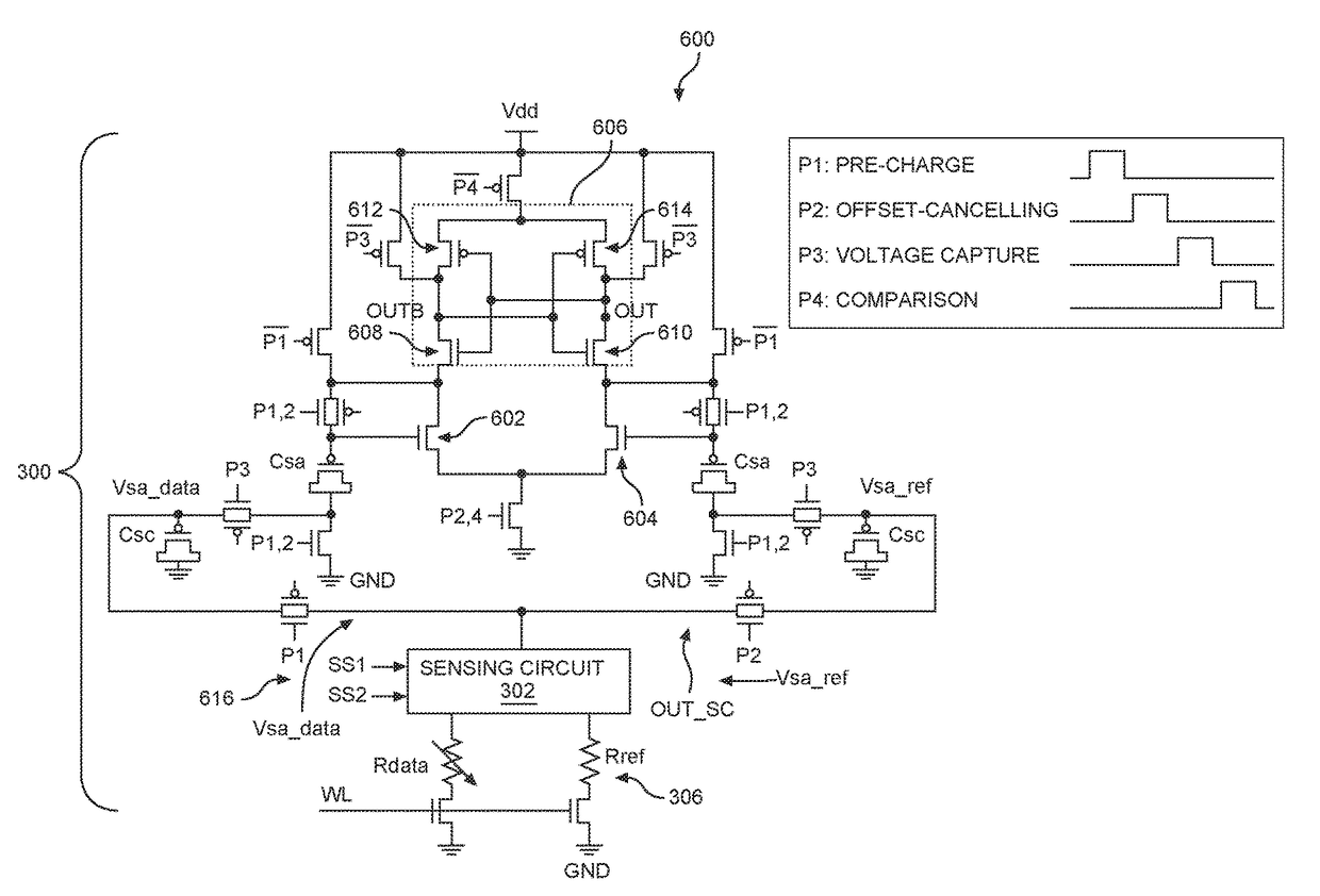
[0033]Aspects of the present disclosure include metal-oxide semiconductor (MOS) transistor offset-cancelling (OC), zero-sensing (ZS) dead zone, current-latched sense amplifiers (SAs) (CLSAs) (OCZS-SAs) for sensing differential voltages. For example, an OCZS-SA may be part of memory read circuitry in a memory system for reading data from a memory array for a read operation. The OCZS-SA may be configured to receive differential data and reference input voltages from a sensing circuit in a resistive memory system indicative of the storage state of a memory bitcell(s). The OCZS-SA is configured to amplify the received differential data and reference input...


PUM


Abstract

Metal-oxide semiconductor (MOS) transistor offset-cancelling (OC), zero-sensing (ZS) dead zone, current-latched sense amplifiers (SAs) (CLSAs) (OCZS-SAs) for sensing differential voltages are provided. An OCZS-SA is configured to amplify received differential data and reference input voltages with a smaller sense amplifier offset voltage to provide larger sense margin between different storage states of memory bitcell(s). The OCZS-SA is configured to cancel out offset voltages of input and complement input transistors, and keep the input and complement input transistors in their activated state during sensing phases so that sensing is not performed in their “dead zones” when their gate-to-source voltage (Vgs) is below their respective threshold voltages. In other aspects, sense amplifier capacitors are configured to directly store the data and reference input voltages at gates of the input and complement input transistors during voltage capture phases to avoid additional layout area that would otherwise be consumed with additional sensing capacitor circuits.

Description

BACKGROUNDI. Field of the Disclosure[0001]The technology of the disclosure relates generally to magnetic random access memories (MRAMs) comprising MRAM bitcells for storing data as a function of magnetic polarization of magnetic tunnel junction (MTJ) storage elements, and more particularly to sensing circuitry for sensing storage states of MRAM bitcells as part of a read operation.II. Background[0002]Semiconductor storage devices are used in integrated circuits (ICs) in electronic devices to provide data storage. One example of a semiconductor storage device is magnetic random access memory (MRAM). MRAM is non-volatile memory in which data is stored by programming a magnetic tunnel junction (MTJ) as part of an MRAM bitcell. Unlike conventional random access memory (RAM) chip technologies, in MRAM, data is not stored as an electric charge, but is instead stored by magnetic polarization of storage elements. Thus, one advantage of an MRAM is that the MRAM bitcells can retain stored inf...

Claims


Application Information

Patent Timeline
Patent Type & Authority Patents(United States)
IPC IPC(8): G11C11/16
CPCG11C11/1673G11C11/161G11C11/1697G11C7/065G11C7/08G11C2207/002G11C2207/063
Inventor NA, TAEHUISONG, BYUNG KYUJUNG, SEONG-OOKKIM, JUNG PILLKANG, SEUNG HYUK
Owner QUALCOMM TECHNOLOGIES INC
Why Eureka
Try Eureka