
Light-emitting device comprising partition including overhang portion

a technology of light-emitting devices and partitions, which is applied in the direction of semiconductor devices, solid-state devices, diodes, etc., can solve the problems of large current flow, crosstalk phenomenon, deterioration of organic el elements, etc., and achieve the suppression of crosstalk phenomenon, wide process margin, and suppressed occurrence of crosstalk phenomenon

Active Publication Date: 2017-08-08
SEMICON ENERGY LAB CO LTD +1
View PDF144 Cites 1 Cited by
  • Summary
  • Abstract
  • Description
  • Claims
  • Application Information

AI Technical Summary

Benefits of technology

This design effectively reduces crosstalk occurrences, allowing for higher luminance with lower current density while maintaining the longevity of tandem light-emitting elements by ensuring electrical isolation and uniform potential across electrodes.

Problems solved by technology

However, a large current flow accelerates deterioration of organic EL elements.
One problem of a light-emitting panel in which tandem elements are provided adjacently is occurrence of a crosstalk phenomenon.

Method used


Image

  • Light-emitting device comprising partition including overhang portion
  • Light-emitting device comprising partition including overhang portion
  • Light-emitting device comprising partition including overhang portion

Examples


embodiment 1

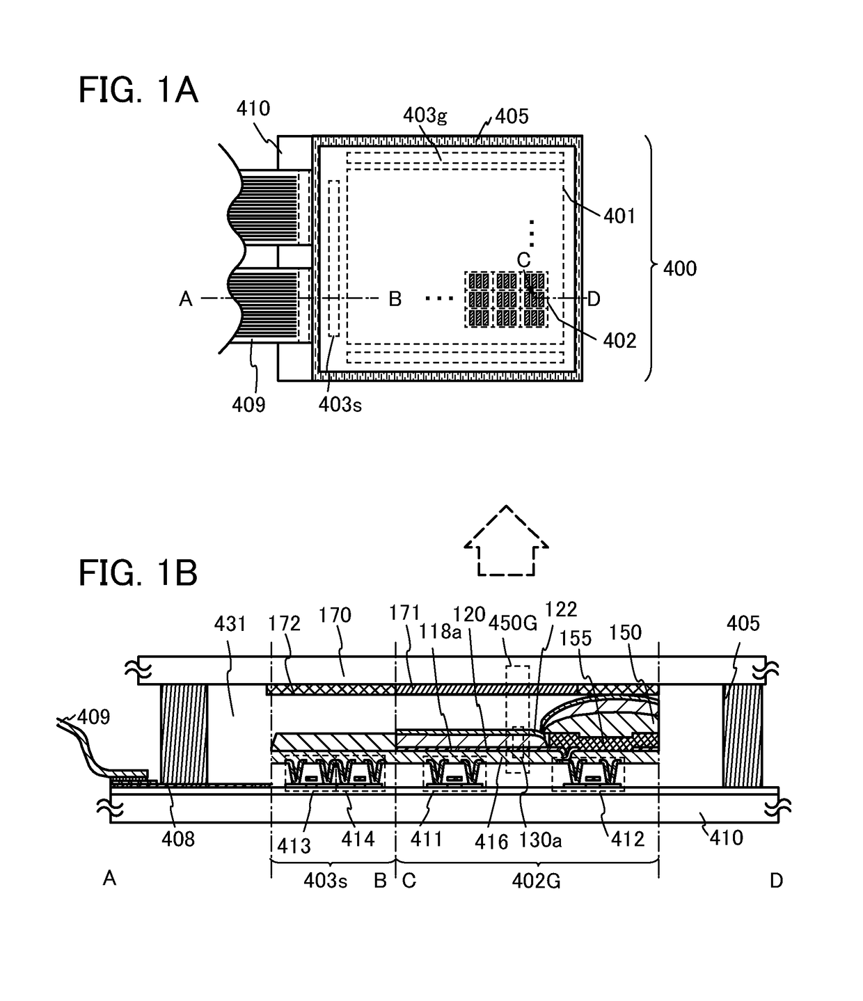
[0052]FIGS. 1A and 1B illustrate a structure of a display panel which can be used for a display device in one embodiment of the present invention. FIG. 1A is a top view of the structure of the display panel which can be used for a display device in one embodiment of the present invention, and FIG. 1B is a side view of the structure including cross sections along section lines A-B and C-D in FIG. 1A.

[0053]A display panel 400 shown as an example in this embodiment includes a display portion 401 over a first substrate 410. The display portion 401 includes a plurality of pixels 402. The pixel 402 includes a plurality of sub-pixels (e.g., three sub-pixels) (see FIG. 1A). Over the first substrate 410, in addition to the display portion 401, a source side driver circuit portion 403s and a gate side driver circuit portion 403g which drive the display portion 401 are provided. Note that the driver circuit portions can be provided not over the first substrate 410 but externally.

[0054]The disp...

example 1

[0123]Lower electrode: silver, silver-magnesium alloy, indium tin oxide (ITO), or metal oxide in which indium is mixed with zinc oxide

[0124]Conductive sacrifice layer: Al or Al alloy

[0125]Etchant: photoresist developer (alkali metal such as tetramethyl ammonium hydroxide (TMAH))

[0126]Partition: acrylic-based resin, polyimide-based resin, siloxane-based resin, phenol-based resin, novolac-based resin, or the like

example 2

[0127]Lower electrode: ITO, Ti oxide, or the like

[0128]Conductive sacrifice layer: indium zinc oxide

[0129]Etchant: oxalic acid etchant

[0130]Partition: acrylic-based resin, polyimide-based resin, siloxane-based resin, phenol-based resin, novolac-based resin, or the like


PUM


Abstract

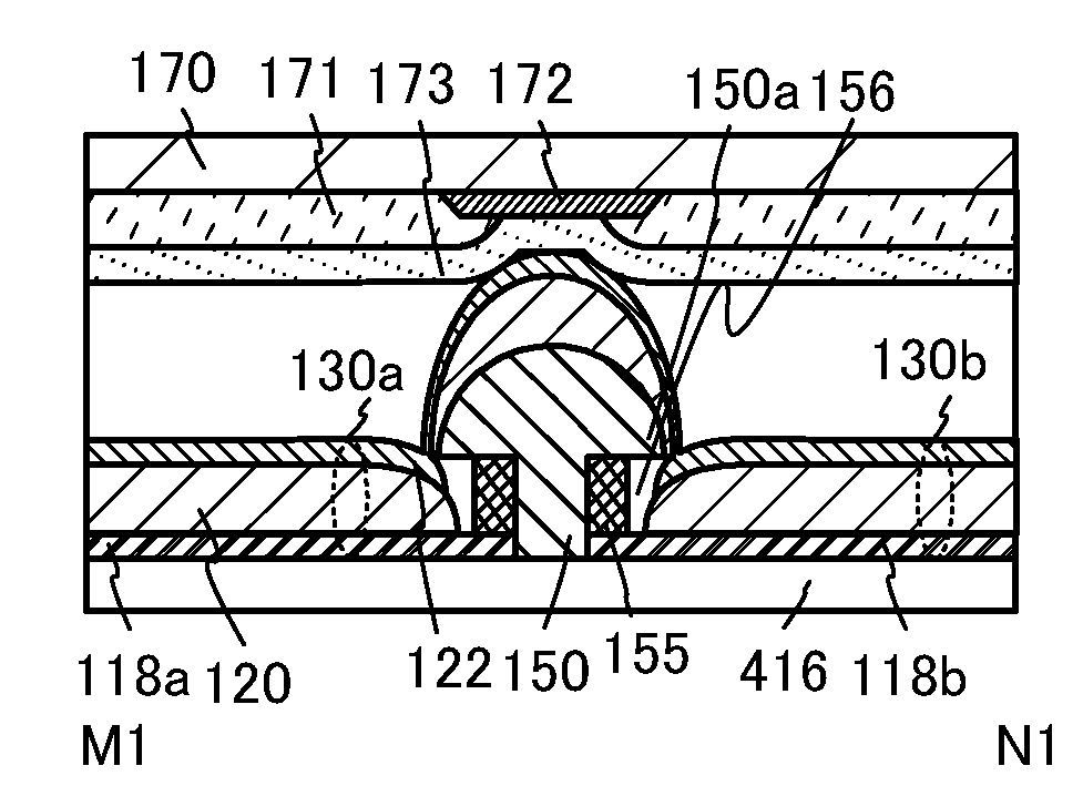
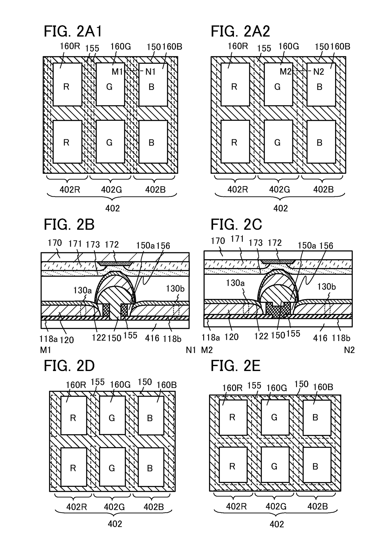
Occurrence of a crosstalk phenomenon in a light-emitting device including a tandem element is suppressed. A light-emitting device includes: lower electrodes over an insulating layer; a partition over a portion between the lower electrodes, which includes an overhang portion over an end portion of each of the lower electrodes; a first light-emitting unit over each of the lower electrodes and the partition; an intermediate layer over the first light-emitting unit; a second light-emitting unit over the intermediate layer; and an upper electrode over the second light-emitting unit. The distance between the overhang portion and each of the lower electrodes is larger than the total thickness of the first light-emitting unit and the intermediate layer over the lower electrode.

Description

BACKGROUND OF THE INVENTION[0001]1. Field of the Invention[0002]One embodiment of the present invention relates to a light-emitting device including a tandem element and a method for manufacturing the light-emitting device.[0003]2. Description of the Related Art[0004]Commercialization of organic EL displays is accelerating. Displays are increasingly required to provide high luminance for outdoor use. It is known that the luminance of an organic EL element increases in proportion to electric current and light emission at high luminance can be achieved.[0005]However, a large current flow accelerates deterioration of organic EL elements. Thus, if high luminance can be achieved with a small amount of current, light-emitting elements can have longer lifetime. In this regard, a tandem element in which a plurality of light-emitting units is stacked has been proposed as a light-emitting element capable of providing high luminance with a small amount of current (see Patent Document 1, for ex...

Claims


Application Information

Patent Timeline
Patent Type & Authority Patents(United States)
IPC IPC(8): H01L27/15H01L33/62H01L33/00H01L51/50H01L51/52H01L27/32
CPCH01L33/62H01L27/3246H01L33/005H01L51/5044H01L51/5278H01L27/322H01L27/3209H01L2924/0002H01L2924/00H10K59/38H10K59/122H10K50/131H10K50/19H10K59/32
Inventor HATANO, KAORUHAMADA, TAKASHIMIYATA, KIKUOKATSUI, HIROMITSUOKAZAKI, SHOJI
Owner SEMICON ENERGY LAB CO LTD
Learn More