
MEMS sensor

a technology of inertial measurement and sensor, which is applied in the direction of microstructural devices, microstructure systems, coatings, etc., can solve the problems of increasing the cost and complexity of the semiconductor device manufacturing process, the current monolithic harpss fabrication process requires significantly complex and difficult process steps, and the widespread use of industries, so as to reduce the size of the device, reduce the amount of release etching, and the effect of sensitivity to the desired motion

Active Publication Date: 2017-07-25
PANASONIC CORP
View PDF3 Cites 6 Cited by
  • Summary
  • Abstract
  • Description
  • Claims
  • Application Information

AI Technical Summary

Benefits of technology

The disclosed semiconductor manufacturing process allows for the formation of complex multi-layer, hermetically-sealed MEMS devices without using expensive SOI substrates. It also simplifies the etching process and enables the use of a thicker device layer, which facilitates designs capable of operating with higher-order modes for sensing. Additionally, out-of-plane electrodes are formed both above and below the MEMS device layer to enhance sensitivity and reduce spurious signals. Overall, the process improves the efficiency and performance of inertial measurement MEMS semiconductor devices.

Problems solved by technology

Inertial measurement devices, such as gyroscopes and accelerometers, provide high-precision sensing, however, historically, their cost, size, and power requirements have prevented their widespread use in industries such as consumer products, gaming devices, automobiles, and handheld positioning systems.
The current monolithic HARPSS fabrication process requires significantly complex and difficult process steps to create all the features necessary for a multi-axis gyro and accelerometer sensor.
However, such as SOI technology increases the cost and complexity of the semiconductor device manufacturing process.

Method used


Image

  • MEMS sensor
  • MEMS sensor
  • MEMS sensor

Examples


Embodiment Construction

[0035]The present disclosure will be more completely understood through the following description, which should be read in conjunction with the drawings. The skilled artisan will readily appreciate that the methods, apparatus and systems described herein are merely exemplary and that variations can be made without departing from the spirit and scope of the disclosure.

[0036]Technologies disclosed herein are directed towards sensing rotation and acceleration around all three axes of free space using an inertial measurement MEMS device. Such devices may have six degrees of freedom in their mechanical design to be able to sense six independent motion signals, i.e. linear acceleration along and angular velocity signals around three orthogonal axes of free space. The manufacturing techniques and designs disclosed herein may be used with any number of commercially available MEMS gyroscopes including those disclosed in the previously mentioned U.S. Pat. No. 7,023,065 United States Patent Ap...

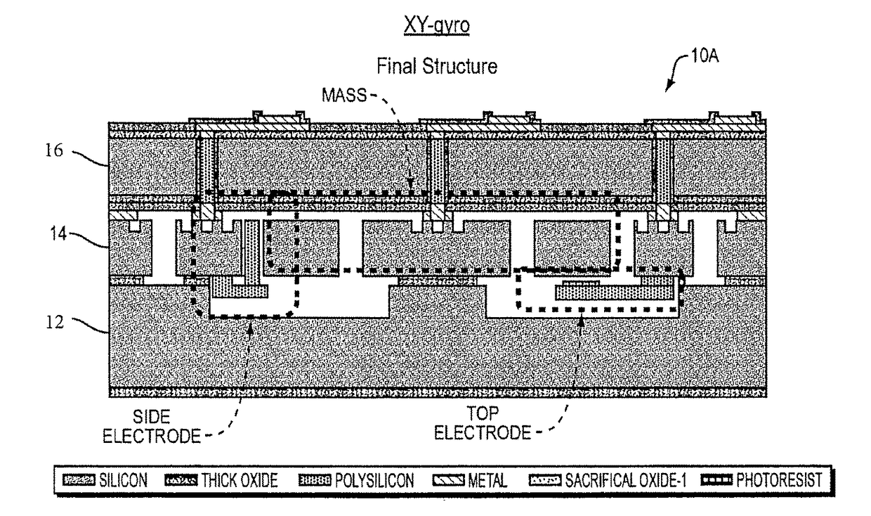
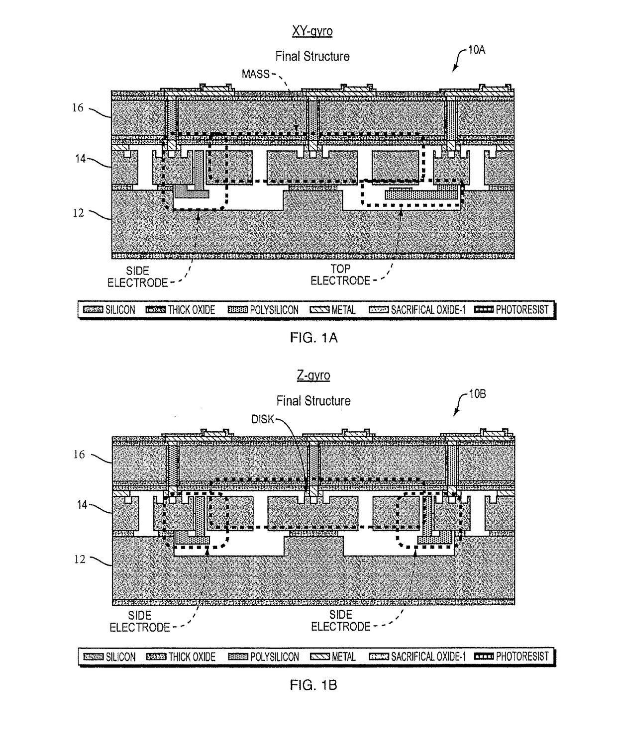
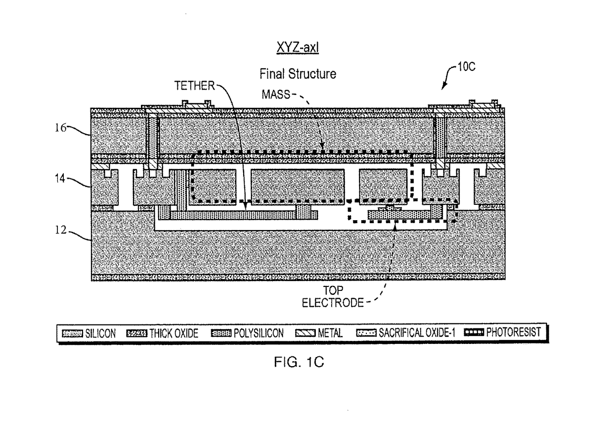

PUM

PropertyMeasurementUnit
massaaaaaaaaaa
thicknessaaaaaaaaaa
sizeaaaaaaaaaa

Abstract

A semiconductor manufacturing process enables a complex multi-layer, silicon based MEMS devices, such as a gyroscope or accelerometer to be formed without using Silicon On Insulator (SOI) substrates and obviates the need to purchase and use SOI wafers as starting materials. The disclosed techniques further allows the etching of the sacrificial oxide to be “head started” prior to fusion bonding, thereby reducing the amount of release etching required at the end of the MEMS wafer processing.

Description

FIELD OF THE INVENTION[0001]The disclosure relates to an alternate process for manufacturing inertial measurement devices that results in a reduction of size and cost of the manufactured product.BACKGROUND OF THE INVENTION[0002]Inertial measurement devices, such as gyroscopes and accelerometers, provide high-precision sensing, however, historically, their cost, size, and power requirements have prevented their widespread use in industries such as consumer products, gaming devices, automobiles, and handheld positioning systems.[0003]More recently, micro-electro-mechanical systems (MEMS) devices, such as gyroscopes and accelerometers, have been gaining increased attention from multiple industries since micro-machining technologies have made fabrication of miniature gyroscopes and accelerometers possible. Miniaturization also enables integration of MEMS devices with readout electronics on the same die, resulting in reduced size, cost, and power consumption as well as improved resolutio...

Claims


Application Information

Patent Timeline
Patent Type & Authority Patents(United States)
IPC IPC(8): H01L23/00B81B3/00B81C1/00
CPCB81B3/0021B81C1/00523B81B2201/0235B81B2201/0242B81B2203/04B81C1/00182B81C1/00301B81B2201/025B81B2207/095B81C2201/019B81C2203/0118
Inventor HRUDEY, PETER CHARLES PHILIP
Owner PANASONIC CORP
Learn More