Image sensor, image capturing apparatus, and cellular phone

a technology of image sensor and image sensor, which is applied in the field of image sensor and image capture apparatus and cellular phone, can solve the problems of increasing mechanical design load, image sensor interference with the light path of the optical viewfinder of the single-lens reflex camera, and large area of the peripheral circuit, so as to achieve high-speed readout operation without excessively increasing the area and cost of an image sensor

Active Publication Date: 2017-04-11
CANON KK
View PDF9 Cites 1 Cited by
  • Summary
  • Abstract
  • Description
  • Claims
  • Application Information

AI Technical Summary

Benefits of technology

[0013]The present invention has been made in consideration of the above situation, and achieves a high quality image and a high-speed readout operation without excessively increasing the area and cost of an image sensor.

Problems solved by technology

If A / D converters are added as peripheral circuits as described in Japanese Patent Laid-Open No. 05-048460, however, the area of the peripheral circuits unwantedly becomes relatively large as the functions of the peripheral circuits increase.
Especially when incorporating an image sensor in a single-lens reflex camera, if the size in the vertical direction of the image sensor (the size in the vertical direction of the camera) increases, the image sensor interferes with the light path of the optical viewfinder of the single-lens reflex camera.
This requires the conventional mechanical structure of the single-lens reflex camera to be largely modified, and thus the load of mechanical design increases.
Even if modification is implemented, a large viewfinder prism and the like become necessary, thereby increasing the cost of the mechanical structural parts and optical parts.
In fact, however, in a single-lens reflex digital camera using a large-capacity memory, it is necessary to arrange a memory chip near the image processing block, and thus it is not always desirable to arrange the image processing block on the second chip.
If the image signal processing block is not arranged on the second chip, the number of circuits actually arranged on the second chip is very small with respect to the chip area, resulting in a very expensive stacked chip.

Method used


Image

  • Image sensor, image capturing apparatus, and cellular phone
  • Image sensor, image capturing apparatus, and cellular phone
  • Image sensor, image capturing apparatus, and cellular phone

Examples


first embodiment

[0026]The first embodiment of the present invention will be described with reference to FIG. 1. FIG. 1 describes the schematic arrangement of an image sensor according to the first embodiment of the present invention. Note that the image sensor of the present invention can be used for various image capturing apparatuses represented by a digital camera, a digital video camera, and the like.

[0027]As shown in FIG. 1, in the image sensor according to the first embodiment, a plurality of pixels 101 are two-dimensionally arranged. Note that FIG. 1 shows six pixels in each of the horizontal direction (row direction) and the vertical direction (column direction) for the sake of descriptive convenience. However, several millions to several tens of millions of pixels 101 are arranged in an actual image sensor. The detailed arrangement of the pixel 101 will be described with reference to FIG. 2.

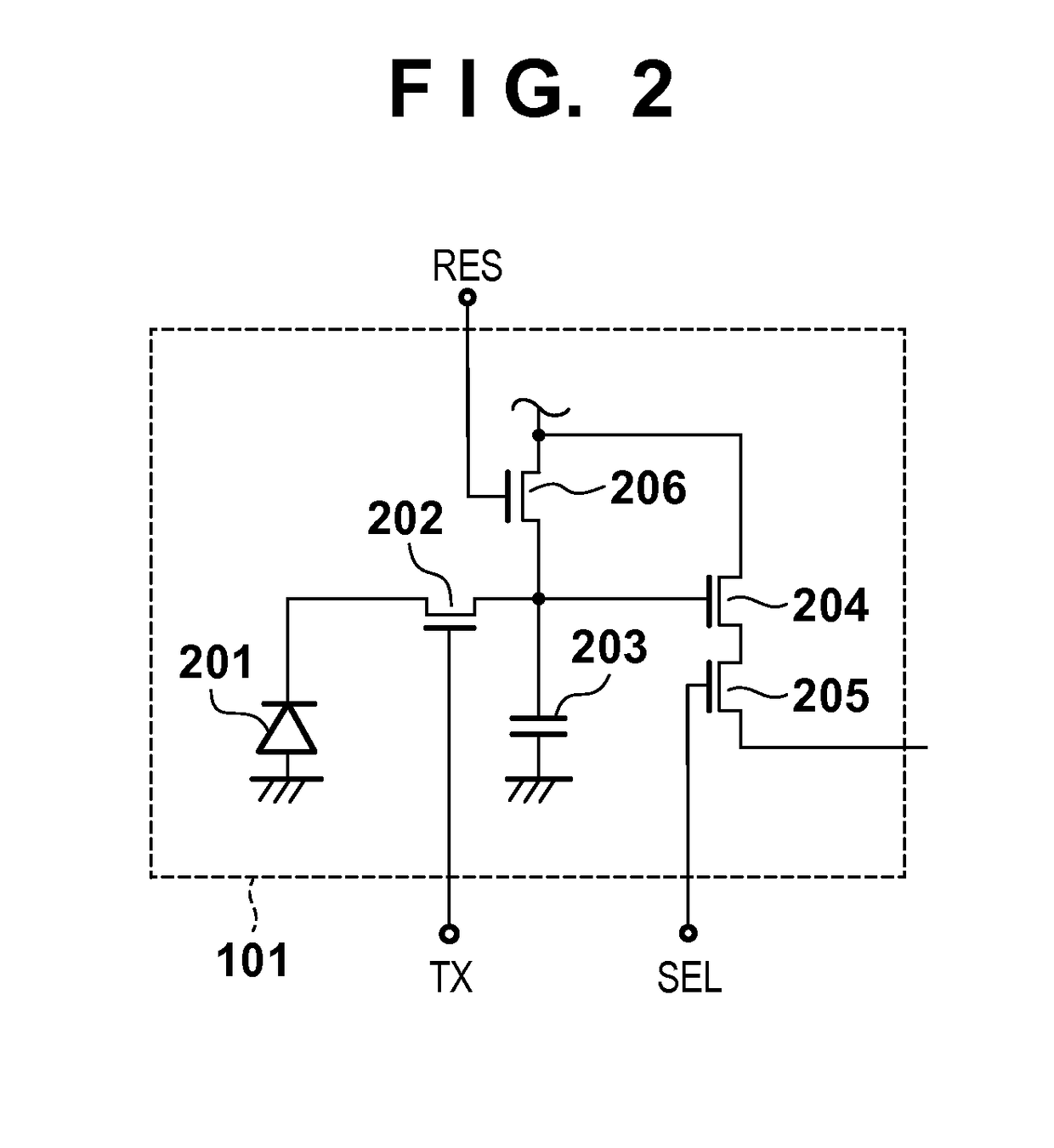
[0028]As shown in FIG. 2, the pixel 101 includes a photodiode 201, a transfer switch 202, a floating...

second embodiment

[0059]An image sensor according to the second embodiment of the present invention will be described below. In the second embodiment, an image sensor in which a vertical output line (column output line) is divided into four lines in the vertical direction (column direction), and the end portion of each line is set as a connection point to the second semiconductor will be explained.

[0060]FIG. 5A is an overlooking view when viewed from the side of a first semiconductor 2111 in which the pixel area of the image sensor is arranged according to the second embodiment. Referring to FIG. 5A, vertical scanning circuits 104a to 104d, signal selection circuits 105a to 105d, a pixel area in which pixels 101 are two-dimensionally arranged, and divided vertical output lines 102a to 102d in the vertical direction on each column are arranged on the first semiconductor 2111. A connection point 113 for electrically connecting to a second semiconductor 2112 is arranged in the end portion of each of the...

third embodiment

[0067]FIG. 6 is a block diagram showing an arrangement of a cellular phone 300 according to the third embodiment of the present invention. The cellular phone 300 according to the third embodiment has the e-mail function, Internet connection function, image shooting / playback function, and the like, in addition to the voice communication function.

[0068]In FIG. 6, a communication unit 301 communicates voice data and image data with another phone by a communication method complying with a communication carrier with which the user has a contract. In voice communication, a voice processing unit 302 converts voice data from a microphone 303 into a format suited for origination, and sends the converted data to the communication unit 301. Also, the voice processing unit 302 decodes voice data from a call destination that has been sent from the communication unit 301, and sends the decoded data to a loudspeaker 304.

[0069]An image sensing unit 305 includes the image sensor described in one of ...


PUM


Abstract

An image sensor comprises: a first semiconductor including a plurality of pixels two-dimensionally arranged, and a plurality of divided output lines, in a first direction, configured to read out pixel signals from the plurality of pixels in the first direction; and a second semiconductor including a plurality of signal processing units, corresponding to the plurality of output lines, respectively, configured to process the readout pixel signals, and a readout unit configured to read out the signals output from the signal processing units in a second direction, wherein the first semiconductor and the second semiconductor are stacked, and the plurality of output lines and the plurality of signal processing units are connected in correspondence with each other.

Description

BACKGROUND OF THE INVENTION[0001]Field of the Invention[0002]The present invention relates to an image sensor, and an image capturing apparatus and cellular phone that use the image sensor.[0003]Description of the Related Art[0004]Conventionally, a CMOS image sensor has been widely adopted for an image capturing apparatus such as a digital camera and digital video camera. The image sensor includes a pixel area, and its peripheral circuits for outputting, amplifying, and reading out signals from the pixel area.[0005]In recent years, along with miniaturization of pixels, it has been considered how to ensure the area of a photodiode. By reducing the number of elements constituting each pixel, it is possible to ensure the area of a photodiode, and also ensure a large number of pixels and image quality.[0006]On the other hand, if only the number of pixels is increased, the readout speed decreases. Therefore, to implement a high-speed readout operation, for example, a plurality of horizon...

Claims


Application Information

Patent Timeline
Patent Type & Authority Patents(United States)
IPC IPC(8): H04N5/374H04N5/3745H04N5/378H04N5/376H01L27/146
CPCH04N5/374H01L27/1464H01L27/14634H01L27/14636H04N5/376H04N5/378H04N5/3742H04N5/37455H04N25/767H04N25/76H04N25/772H04N25/74H04N25/75
Inventor KITANI, KAZUNARI
Owner CANON KK
Why Eureka
Try Eureka