
Amplifier topology for envelope tracking

a topology and amplifier technology, applied in the field of amplifiers and electronic devices, can solve problems such as low efficiency, and achieve the effects of reducing power consumption, low gain variation, and low gain variation

Active Publication Date: 2017-03-21
TELEFON AB LM ERICSSON (PUBL)
View PDF5 Cites 1 Cited by
  • Summary
  • Abstract
  • Description
  • Claims
  • Application Information

AI Technical Summary

Benefits of technology

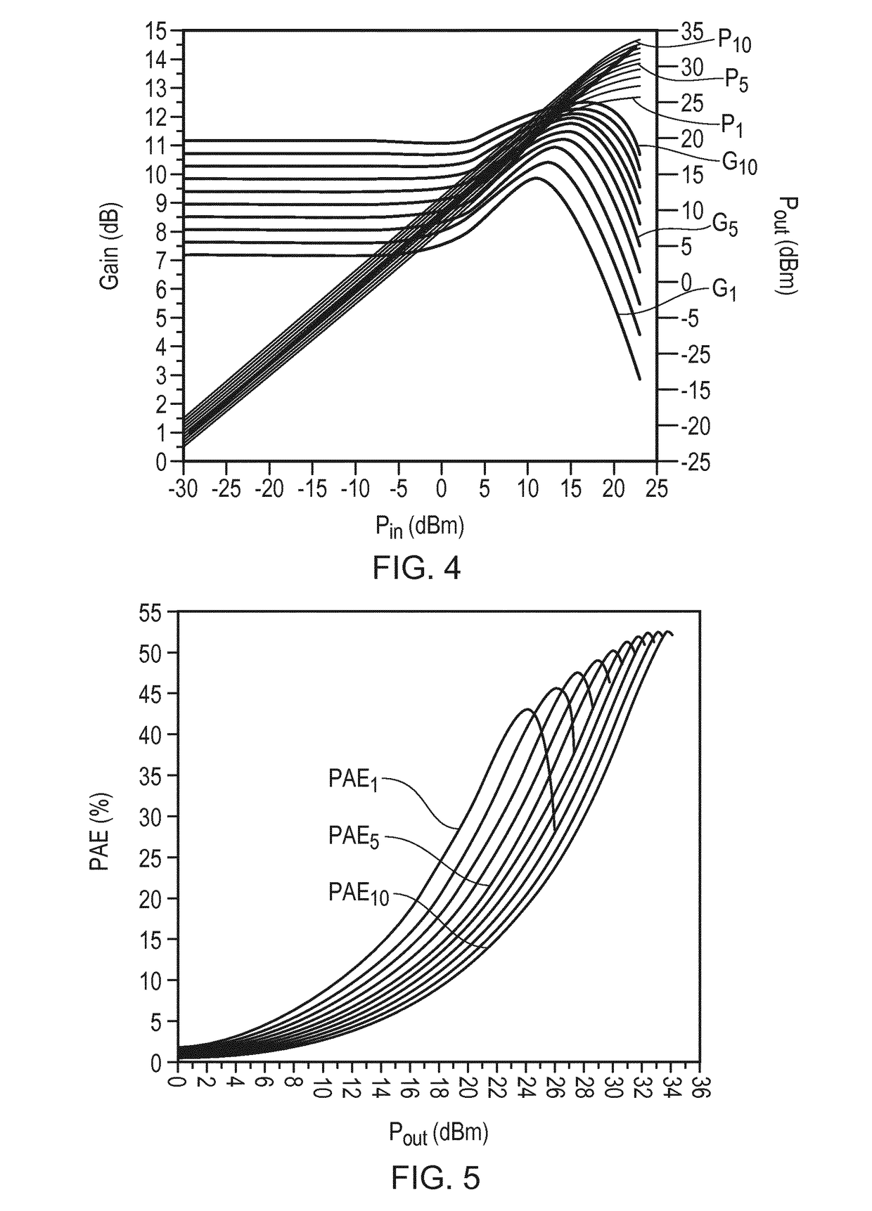
[0022]By employing cascaded transistors for envelope tracking, the amplifier can enable an increased voltage range at the output, with high power efficiency. The use of cascaded transistors can also enable an increased isolation between the output and input of the amplifier, improving stability and reducing the impact on the input impedance of variation in the load impedance, enabling improved linearity. By controlling the bias voltage applied to the gate of each transistor dependent on the envelope signal, such that the bias voltages can track the envelope signal, the amplifier can have a reduced variation in gain as the input power level changes.
[0031]The envelope tracking stage may be arranged to generate the envelope signal quantised to have fewer values than the envelope of the input signal. Likewise, the method of amplification may comprise generating the envelope signal quantised to have fewer values than the envelope of the input signal. This feature can reduce the processing and power consumption.

Problems solved by technology

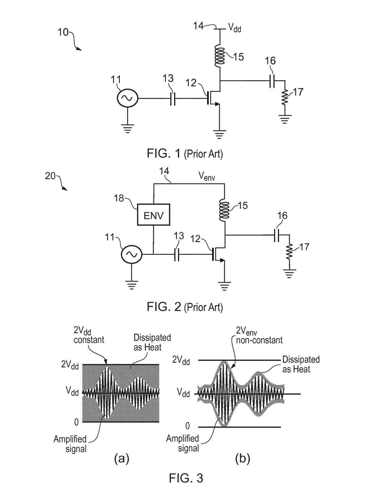
In FIG. 3, the area between the amplified signal and the constant voltage 2Vdd represents power that is unused, not being delivered to the load 17, instead being dissipated as heat, thereby resulting in a low efficiency.

Method used


Image

  • Amplifier topology for envelope tracking
  • Amplifier topology for envelope tracking
  • Amplifier topology for envelope tracking

Examples


first embodiment

[0039]FIG. 6 is an amplifier in accordance with the present disclosure;

[0040]FIG. 7 illustrates load lines for different values of the envelope signal;

[0041]FIG. 8 is a graph of gain and output power as a function of input power for an amplifier with tracking bias voltages in accordance with the present disclosure;

[0042]FIG. 9 is a graph of gain and output power as a function of input power without tracking bias voltages;

[0043]FIG. 10 is a graph of current as a function of output power;

[0044]FIG. 11 is a Smith chart illustrating input impedance;

[0045]FIG. 12 is a graph of Rollet stability factor;

[0046]FIG. 13 is a graph of small signal gain as a function of frequency;

[0047]FIG. 14 is a flow chart of a method of amplification;

[0048]FIG. 15 is a flow chart of a method of calibrating an amplifier;

second embodiment

[0049]FIG. 16 is an amplifier in accordance with the present disclosure; and

[0050]FIG. 17 is a block schematic diagram of an electronic apparatus comprising an amplifier.


PUM


Abstract

An amplifier has an input port for receiving an input signal and an envelope port for receiving an envelope signal indicative of an envelope of the input signal, and an output port for delivering an amplified signal. The amplifier has a first transistor and a second transistor. A first biasing circuit is coupled to the envelope port and is arranged to generate a first bias voltage dependent on the envelope signal. A summing stage is coupled to the input port for receiving the input signal, to the first biasing circuit for receiving the first bias voltage, and to the gate of the first transistor. A second biasing circuit is coupled between the envelope port and the gate of the second transistor, and is arranged to generate a second bias voltage dependent on the envelope signal.

Description

FIELD OF THE DISCLOSURE[0001]The present disclosure relates to an amplifier, and electronic apparatus comprising an amplifier, and a method of amplification.BACKGROUND TO THE DISCLOSURE[0002]Advances in radio technology have led to a demand for a higher level of circuit integration, with different circuits being integrated into a single system on a chip. For example, a radio frequency (RF) front end may include a power amplifier, a low noise amplifier and a switch. Integration of a power amplifier in complementary metal oxide silicon (CMOS) technology can enable a low cost but, for RF usage, such a power amplifier is required to sustain a high power output at a high frequency. Ideally, the power amplifier should combine high power with high efficiency, without efficiency being reduced when the amplifier is operated at low power. One known solution is based on the use of a high efficiency power transistor with power regulation, such as envelope tracking.[0003]Referring to FIG. 1, a b...

Claims


Application Information

Patent Timeline
Patent Type & Authority Patents(United States)
IPC IPC(8): H03F1/22H03F3/193H03F3/24H03F1/02H03F3/19
CPCH03F1/0222H03F1/0266H03F1/223H03F3/19H03F3/193H03F3/245H03F2200/102H03F2200/108H03F2200/15H03F2200/18H03F2200/451
Inventor KNOPIK, VINCENT
Owner TELEFON AB LM ERICSSON (PUBL)
Learn More