Method for the mapping of the local AT/GC ratio along DNA
a technology of at/gc ratio and mapping method, which is applied in the field of mapping method of local at/gc ratio along dna, can solve the problems of inability to use and limit the mapping method, and achieve the effects of low cost, simple method, and short preparation and measurement tim
- Summary
- Abstract
- Description
- Claims
- Application Information
AI Technical Summary
Benefits of technology
Problems solved by technology
Method used
Image
Examples
example
Example 1
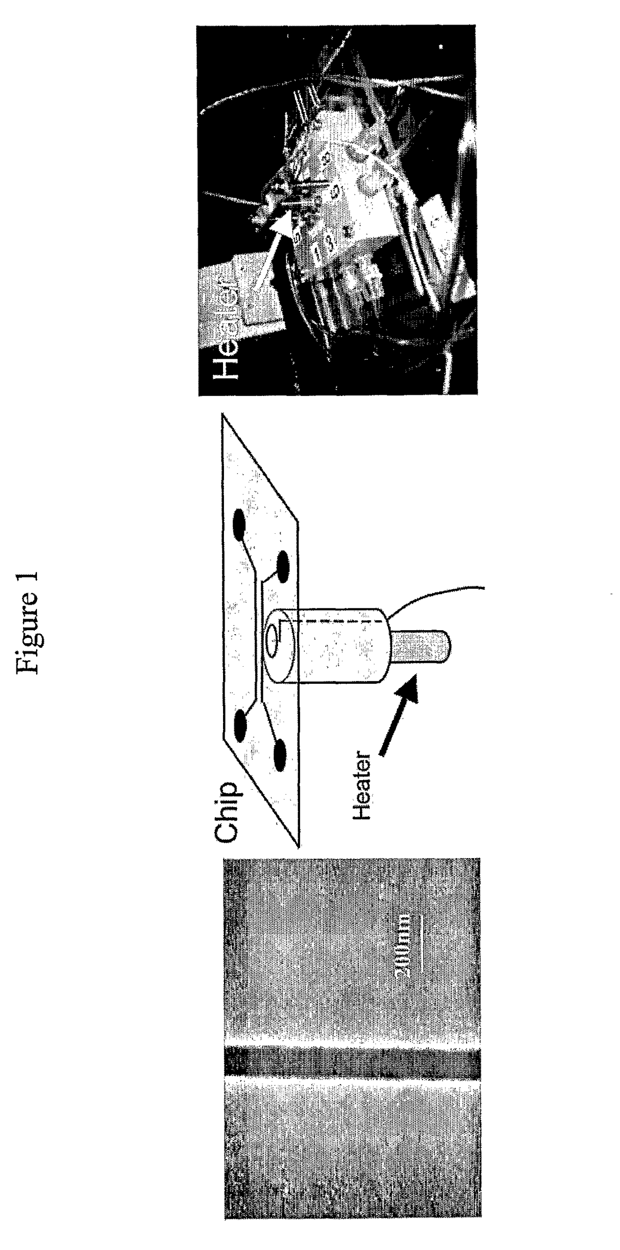
[0060]The device is made in fused silica using standard electron-beam lithography combined with UV-lithography and reactive ion etching. It is placed in a dedicated chuck for temperature control and mounted on an epifluorescence microscope (FIG. 1). Lambda-phage DNA is dyed with a conventional intercalating dye (YOYO-1™ Invitrogen) and dissolved in a buffer with low ionic strength (0.05 TBE+10 mM NaCl) and 33% and 50% formamide respectively to decrease the melting temperature.
Results
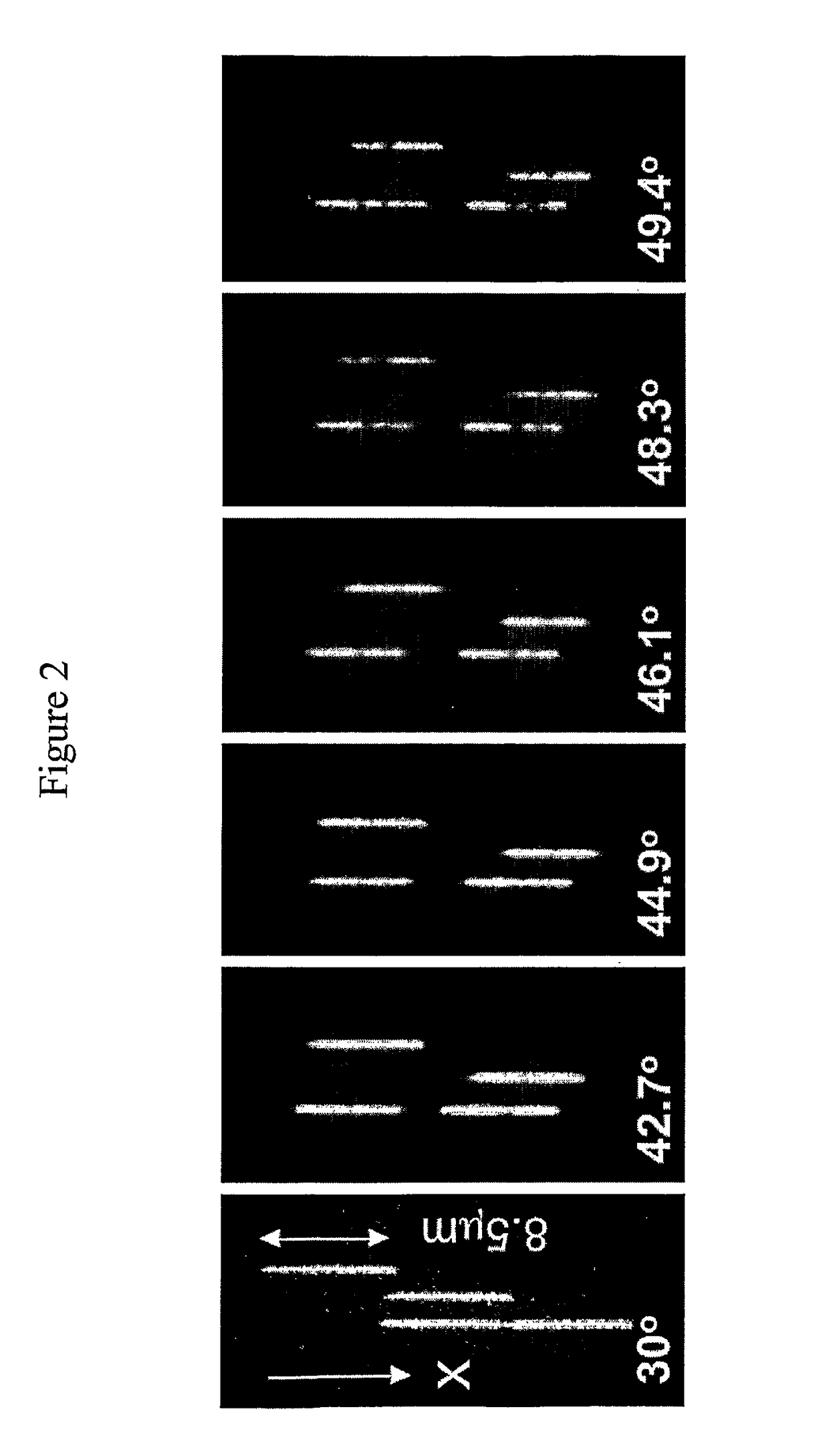
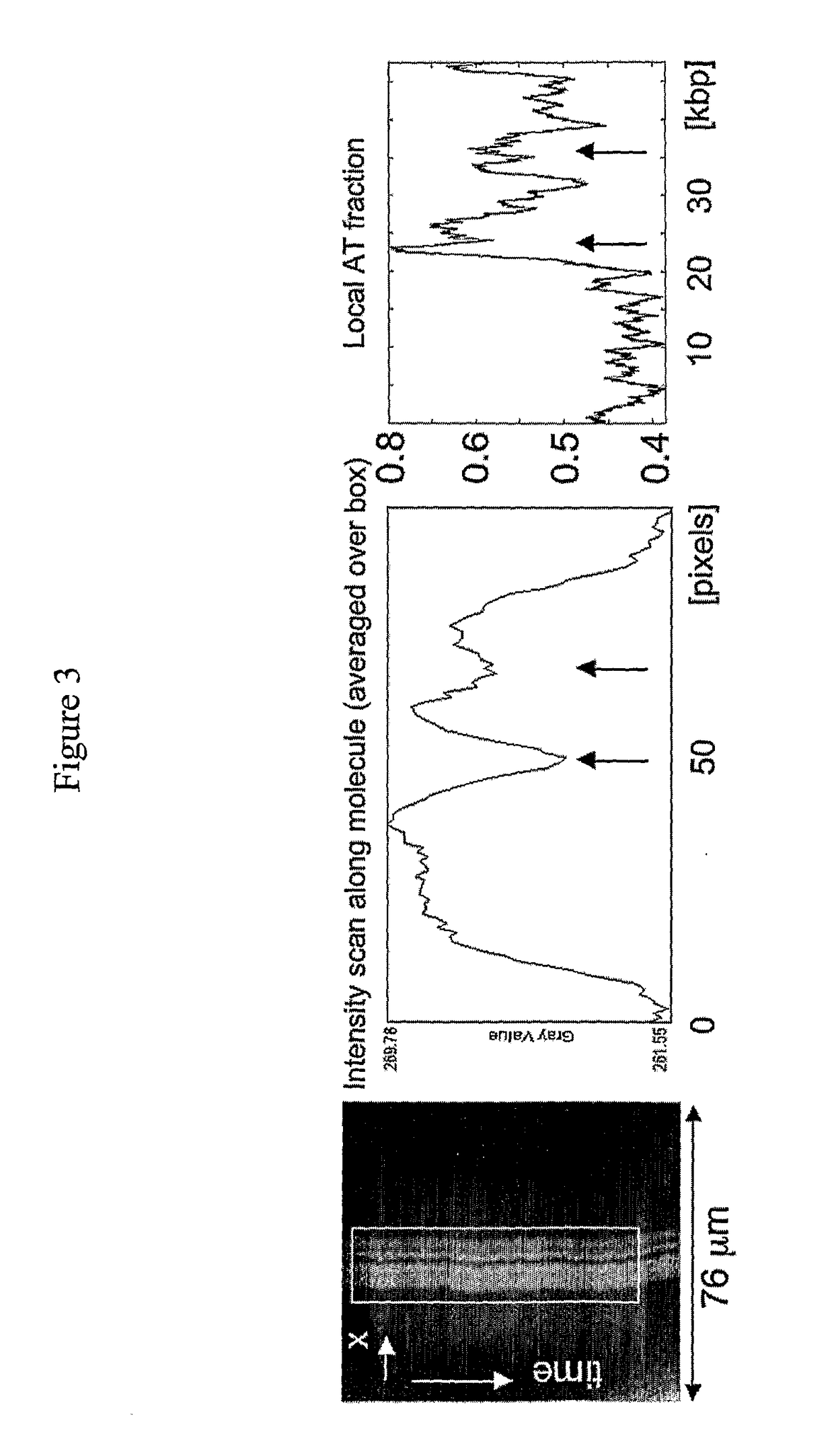
[0061]Uniform fluorescence is seen along each DNA molecule at room-temperature, and with rising temperature, dark patches appear along the DNA corresponding to AT-rich regions that lose in intensity due to local melting of the double-stranded helix thereby resulting in a “barcode” pattern along the DNA. The asymmetric pattern is consistent across all molecules viewed (FIG. 2) and corresponds to AT-rich regions in the middle and on one side of lambda-phage DNA (FIG. 3).
[0062]Gradually increasing ...
example 2
Fabrication
[0064]The devices were fabricated on fused silica wafers (HOYA) via a three stage process combining electron beam and UV contact lithography. A 200 μm long array of 120-150 nm wide nanochannels spaced 2 μm apart was defined using electron beam lithography (JEOL) in zep520A resist and then transferred to the silica substrate via CF4:CHF3 reactive ion etching (RIE). Contact UV lithography was then used to expose a 350 μm long and 50 μm wide nanoslit in photoresist running perpendicular to the nanochannel array. The slit was etched using RIE to a depth of 30 nm. Where the slit and the nanochannel array intersected, an array of nanogroove structures was formed; see FIG. 8. In order to introduce buffer into the nanoslit and nanochannels, a last UV contact lithography and etching step was used to define a 50 μm wide microchannel 1 μm deep in U-shaped arms adjoining the nanoslit and nanochannels (FIG. 8). Loading holes were sandblasted in the reservoirs (eight total) and the chi...
PUM
| Property | Measurement | Unit |
|---|---|---|
| diameter | aaaaa | aaaaa |
| diameter | aaaaa | aaaaa |
| length | aaaaa | aaaaa |
Abstract
Description
Claims
Application Information
 - R&D
- Intellectual Property
- Life Sciences
- Materials
- Tech Scout
- Unparalleled Data Quality
- Higher Quality Content
- 60% Fewer Hallucinations
Browse by: Latest US Patents, China's latest patents, Technical Efficacy Thesaurus, Application Domain, Technology Topic, Popular Technical Reports.
© 2025 PatSnap. All rights reserved.Legal|Privacy policy|Modern Slavery Act Transparency Statement|Sitemap|About US| Contact US: help@patsnap.com


