Semiconductor device

a technology of semiconductor devices and devices, applied in semiconductor devices, semiconductor/solid-state device details, electrical apparatus, etc., can solve the problems of difficult cutting of fuse blades, insufficient protection of upper portions, and difficulty in obtaining a condition that satisfies both requirements, and achieves the effect of expanding the volume of the fuse elemen

Active Publication Date: 2017-01-31
ABLIC INC
View PDF5 Cites 0 Cited by
  • Summary
  • Abstract
  • Description
  • Claims
  • Application Information

AI Technical Summary

Benefits of technology

[0008]The present invention has been made in view of the above-mentioned problems, and provides a semiconductor device including a fuse element that can suppress progress of corrosion from a cut portion of the fuse element.
[0010]According to one embodiment of the present invention, there can be provided a fuse element in which the corrosion due to the penetration of moisture is prevented from progressing inside the semiconductor device as follows. Specifically, after the fuse element is cut by a laser, the sectional area of the fuse element exposed from the cut surface is small, and hence a volume of the fuse element to be expanded is small even if the exposed portion of the fuse element is corroded. Thus, stress to be applied to the fuse protective insulating film is suppressed and the fuse protective insulating film does not crack, which prevents the formation of the new moisture penetration route.

Problems solved by technology

However, because a fuse element is supposed to be cut by laser irradiation later, the silicon nitride film that absorbs the laser cannot be arranged on the fuse element, and hence the protective film formed above the fuse element is removed so as to open the protective film.
However, the above-mentioned related art has the following problems.
Although moisture basically penetrates from a portion above the fuse element from which the protective film is removed, in the method, no moisture resistance insulating film is arranged or the thin moisture resistance insulating film is formed on the upper portion of the fuse element.
Therefore, the protection of the upper portion is insufficient.
Further, because the silicon nitride film or the silicon oxynitride film is used as the moisture resistance insulating film, the radiated laser beam is absorbed, which makes it difficult to cut the fuse.
It is considered that obtaining a condition that satisfies both requirements is difficult to achieve.
This is because, when the fuse element is cut, the fuse element is exposed from the cut surface to cause corrosion.
The fuse element is corroded from the cut surface and the fuse element thus expands, resulting in cracking of the insulating film formed on the fuse element.
Further, a problem arises in that the crack becomes a penetration route of the moisture, and hence the corrosion progresses inside the semiconductor device.

Method used


Image

  • Semiconductor device
  • Semiconductor device
  • Semiconductor device

Examples


first embodiment

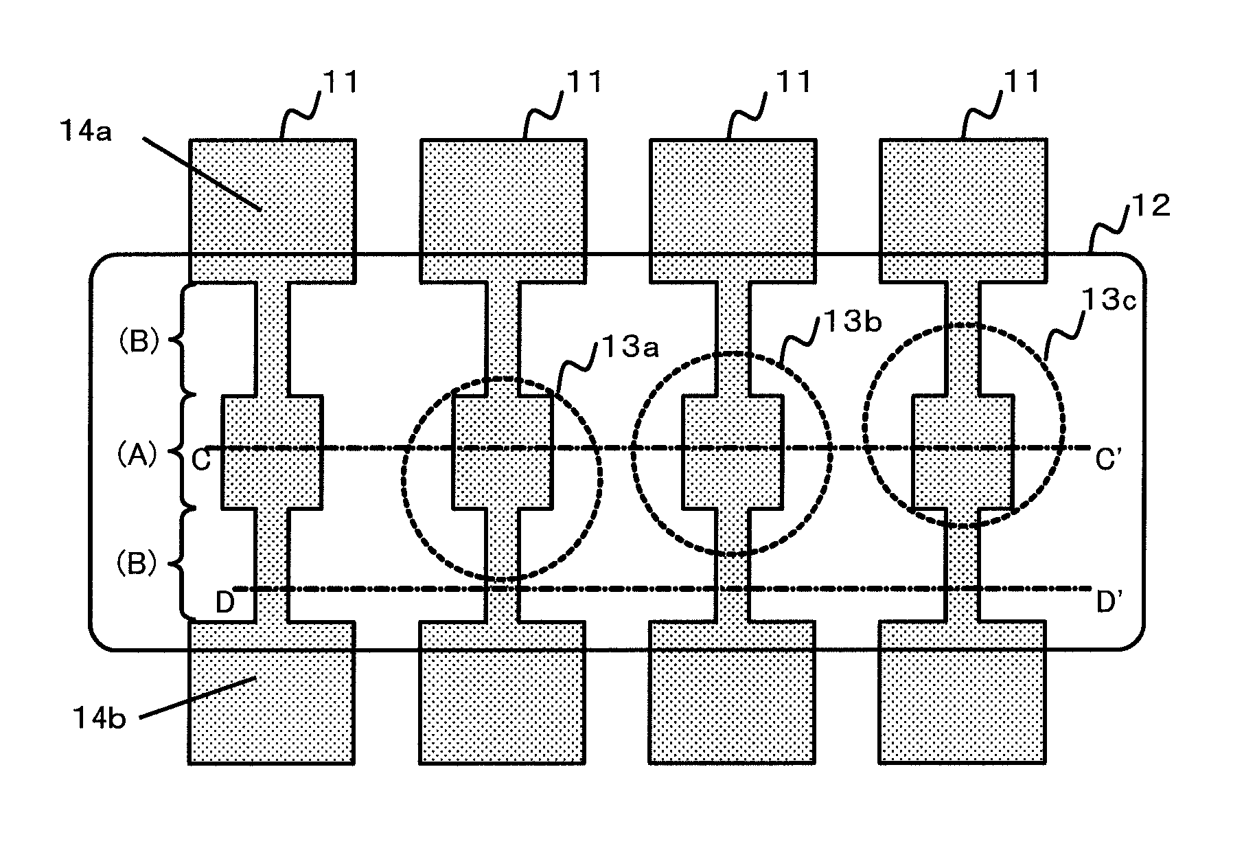
[0018]FIG. 1 is a plan view illustrating a semiconductor device according to a first embodiment of the present invention. A plurality of fuse elements 11 are arranged in parallel, and both ends of each of the fuse elements 11 correspond to first terminals 14a and second terminals 14b, respectively. The respective fuse elements are connected to a circuit via the first and second terminals 14a and 14b. The circuit determines whether or not a current flows between the terminals 14a and 14b. At the fuse element 11 that is not cut, the current flows between the terminals 14a and 14b. A dimension of the fuse element in a direction perpendicular to the current flow is referred to as a width of the fuse element. In FIG. 1, a direction perpendicular to a direction connecting the terminals 14a and 14b corresponds to the width of the fuse element.

[0019]A fuse insulating protective film opening region 12 is arranged on a region including the centers of the fuse elements 11 in order to perform c...

second embodiment

[0026]Next, a semiconductor device according to a second embodiment of the present invention is described with reference to the drawings.

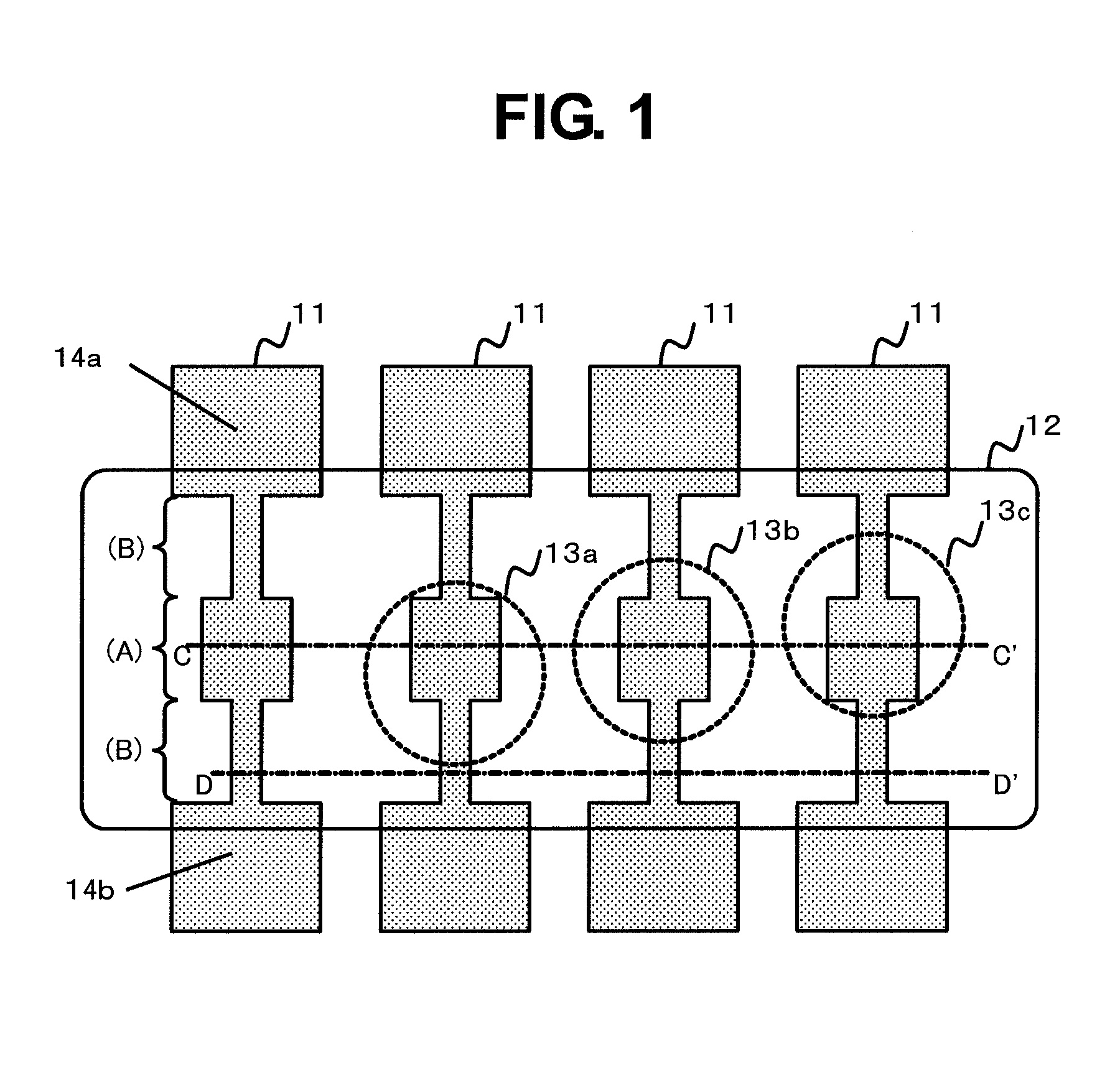
[0027]FIG. 3 is a plan view illustrating the semiconductor device according to the second embodiment of the present invention. The fuse elements 11 are arranged, and the fuse protective insulating film opening region 12 is arranged over the centers of the fuse elements 11 in order to perform the cutting by the laser. The fuse protective insulating film opening region 12 is a region from which the protective film, for example, a silicon nitride film arranged on the upper portion of the semiconductor device is removed. Further, the fuse element 11 includes two regions of the large sectional area region (A) and the small sectional area region (B) as illustrated in FIG. 3.

[0028]The large sectional area regions (A) correspond to thick portions of the fuse elements 11 and are portions to be irradiated with the laser spots 13 when the cutting by the laser...

third embodiment

[0033]Next, a semiconductor device according to a third embodiment of the present invention is described with reference to the drawings.

[0034]This embodiment is a modified example of the second embodiment. As illustrated in FIG. 5, a planar structure of the semiconductor device according to the third embodiment of the present invention is the same as that of FIG. 3. That is, the semiconductor device includes the fuse element 11 including the thick portion and the thin portion. However, as illustrated in FIGS. 6A, 6B, and 6C, the semiconductor device of this embodiment has a different structure from that of the second embodiment in a sectional view.

[0035]FIG. 6A is a sectional view taken along the line C-C′ of FIG. 5, illustrating the thick portion. The insulating film 22 is formed on the silicon substrate 21, and trenches 24 are formed in the insulating film 22. Each of the trenches 24 is filled with a conductive film, to thereby form a part of the thick portions of the respective f...


PUM


Abstract

A semiconductor device includes a fuse element that can be cut and removed by laser irradiation. The fuse element has a large width portion having a large sectional area to be irradiated with a laser spot, and two small width portions having a small sectional area connected to opposite sides of the large width portion. Penetration of moisture is suppressed even after cutting of the fuse element since the large width portion is removed by the laser irradiation and only the small width portions having the small sectional area remain as exposed cut surfaces.

Description

BACKGROUND OF THE INVENTION[0001]1. Field of the Invention[0002]The present invention relates to a semiconductor device, in particular, a semiconductor device including a fuse element that can be cut for changing a circuit configuration of the semiconductor device.[0003]2. Description of the Related Art[0004]There is a method of changing a circuit configuration of a semiconductor device by cutting, in a semiconductor device manufacturing process, a fuse element formed of polysilicon, metal, and the like by using, for example, a laser after a wafer manufacturing process is finished. By using this method, a resistance value can be corrected to obtain desired characteristics after electrical characteristics of the semiconductor device are measured. This method is thus effective particularly for a semiconductor device that places emphasis on its analog characteristics.[0005]In this method, it is required for the fuse element to be stably cut by the laser and have a high corrosion resist...

Claims


Application Information

Patent Timeline
Patent Type & Authority Patents(United States)
IPC IPC(8): H01L23/525
CPCH01L23/5258H01L2924/0002H01L2924/00H01L23/5256H01L23/62
Inventor KITAJIMA, YUICHIRO
Owner ABLIC INC
Why Eureka
Try Eureka