High heat-dissipation chip package structure

Active Publication Date: 2016-10-18
GREAT TEAM BACKEND FOUNDRY (DONGGUAN) LTD
View PDF1 Cites 2 Cited by
  • Summary
  • Abstract
  • Description
  • Claims
  • Application Information

AI Technical Summary

Benefits of technology

The present invention provides a way to package semiconductor chips in a way that helps with heat dissipation and electrical conductivity, while also improving the quality of the fabrication and packaging process. This is done by using a pre-attachment film that is first adhered to a heat-dissipation plate or connection plate, before packaging the chips. After packaging, the film is torn off and a metal layer is electroplated to the area where the film was torn off, all in an effort to improve the overall quality and efficiency of the chip packaging process.

Problems solved by technology

But the chip 3 has worse effect of heat dissipation due to being packaged in the potting compound 4 so that the chip 3 is easily damaged.
However, the potting compound 4 on the heat dissipation plate 5 cannot totally be cleaned and the effect of heat dissipation may be blocked and is still not good enough.

Method used


Image

  • High heat-dissipation chip package structure
  • High heat-dissipation chip package structure
  • High heat-dissipation chip package structure

Examples


Embodiment Construction

[0019]Referring now to the drawings where like characteristics and features among the various figures are denoted by like reference characters.

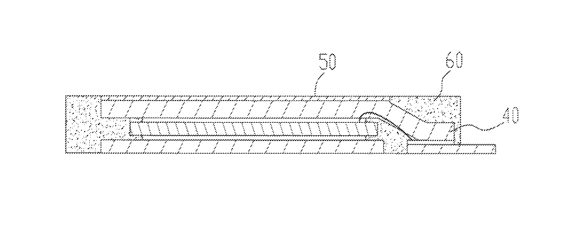
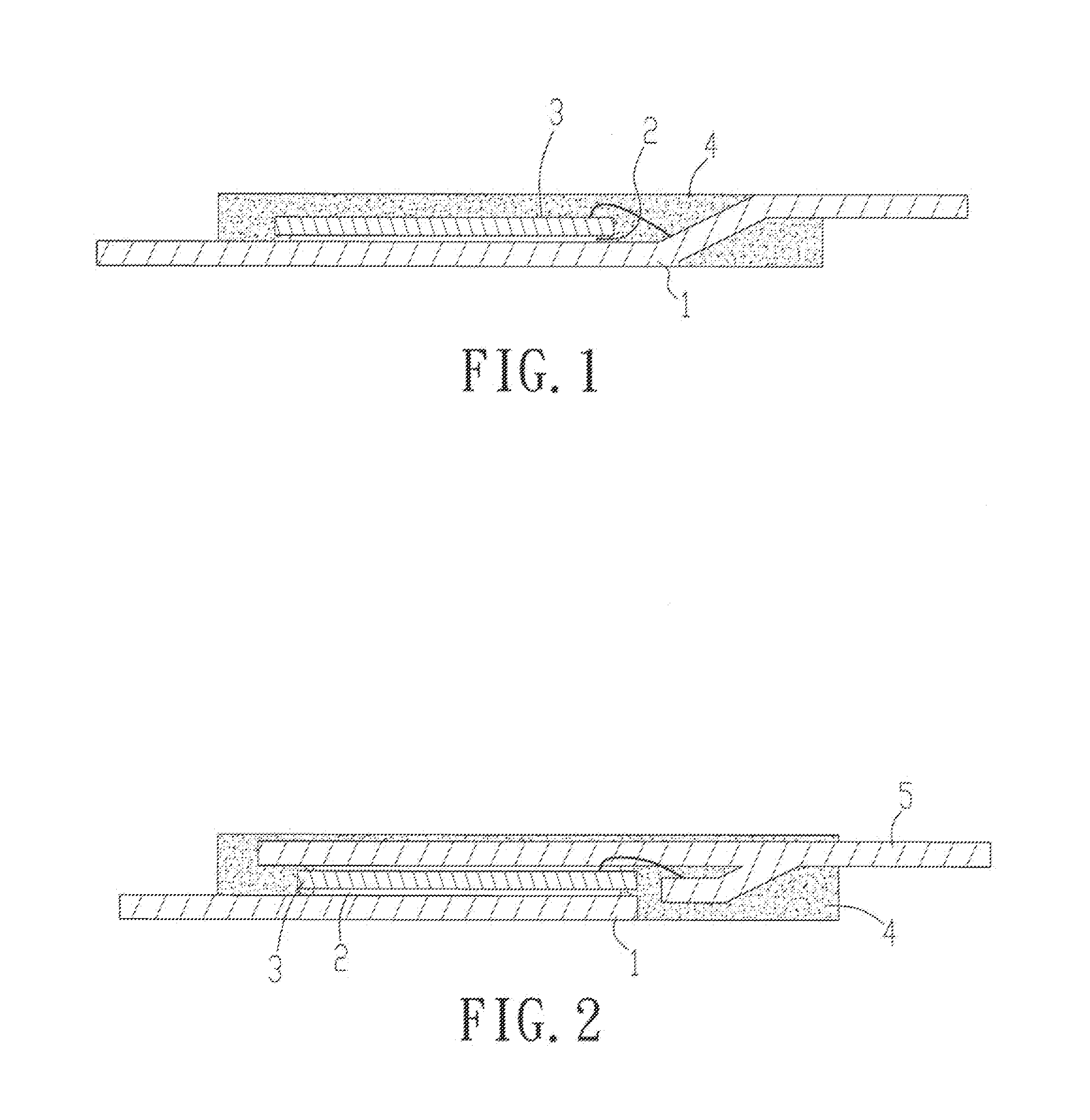
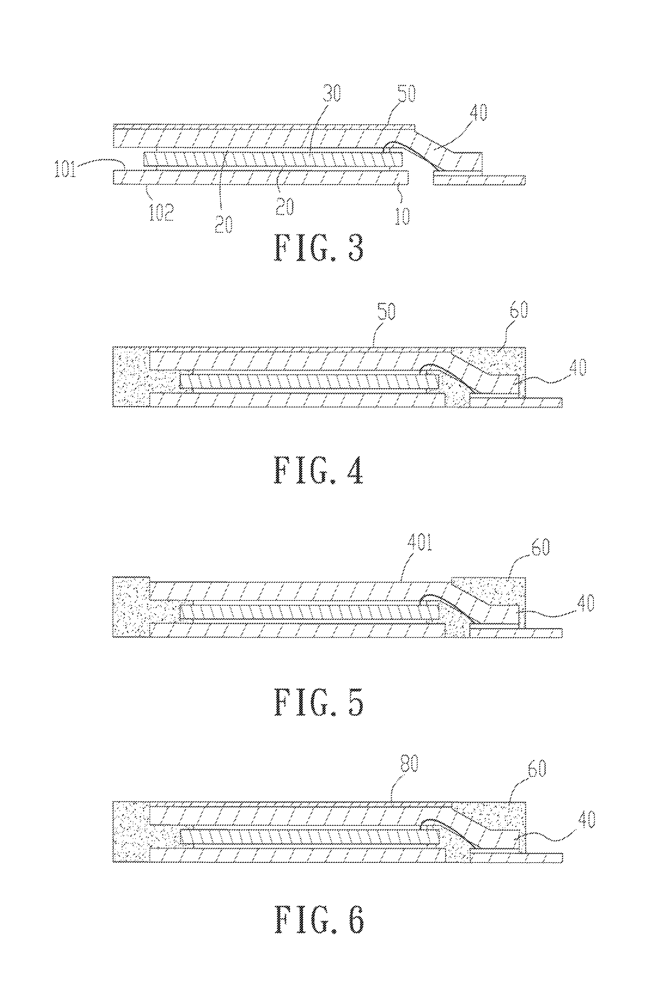
[0020]Please refer to FIGS. 3 to 6, the high heat-dissipation chip package structure of the present invention comprises a base 10, a semiconductor chip 30, a connection plate 40, a pre-attachment film 50, and a potting compound 60.

[0021]The base 10 may have an upper surface 101 and lower surface 102 opposite to each other. An adhesive layer 20 may be coated on the upper surface 101 for adhering the semiconductor chip on the base 10.

[0022]A bottom part of the semiconductor chip 30 may be adhered on the upper surface 101 of the base 1 via the adhesive layer 20 and a top part of the semiconductor chip 30 may be connected with the connection plate via another one adhesive layer 20.

[0023]The connection plate 40 may be electrically connected with the semiconductor chip 30 and a lead frame (not shown). The pre-attachment film 50 may be adhered on a ...


PUM


Abstract

A high heat-dissipation chip package structure for packaging the semiconductor chips is disclosed. A pre-attachment film is adhered on an upper surface of a heat-dissipation plate or a connection plate first and then it is packaged. After packaging, the pre-attachment film is torn off from the upper surface of the heat-dissipation plate or the connection plate. Finally, a metal layer is electroplated on the location of the upper surface of the heat-dissipation plate or the connection plate where the pre-attachment film is torn off so as to improve the fabricating and packaging quality of the semiconductor chips, reduce the cost of cleaning process, and improve the effects of heat dissipation and electrical conductivity.

Description

FIELD OF THE INVENTION[0001]The present invention relates to a chip package structure, and more particularly to a high heat-dissipation chip package structure for packaging the semiconductor chips. A pre-attachment film is adhered on an upper surface of a heat-dissipation plate or a connection plate first and then it is packaged. After packaging, the pre-attachment film is torn off from the upper surface of the heat-dissipation plate or the connection plate. Finally, a metal layer is electroplated on the location of the upper surface of the heat-dissipation plate or the connection plate where the pre-attachment film is torn off so as to improve the fabricating and packaging quality of the semiconductor chips, reduce the cost of cleaning process, and improve the effects of heat dissipation and electrical conductivity.BACKGROUND OF THE INVENTION[0002]The conventional semiconductor chip structure is shown as FIG. 1. An adhesive layer 2 is coated on the upper surface of the base 1 and t...

Claims


Application Information

Patent Timeline
IPC IPC(8): H01L23/495H01L23/31
CPCH01L23/49568H01L23/49513H01L23/4952H01L23/49541H01L23/3114H01L21/565H01L23/3121H01L23/49548H01L23/49582H01L23/49586H01L24/29H01L24/32H01L24/33H01L24/48H01L24/73H01L2224/2919H01L2224/32245H01L2224/33181H01L2224/48091H01L2224/48247H01L2224/73215H01L2224/73265H01L2924/00014H01L2924/00012H01L2224/45015H01L2924/207H01L2224/45099
Inventor TZU, CHUNG HSING
Owner GREAT TEAM BACKEND FOUNDRY (DONGGUAN) LTD
Why Eureka
Try Eureka