Method of manufacturing semiconductor device

Active Publication Date: 2018-05-10
NICHIA CORP
View PDF5 Cites 0 Cited by
  • Summary
  • Abstract
  • Description
  • Claims
  • Application Information

AI Technical Summary

Benefits of technology

The patent describes a way to make semiconductor devices that can easily dissipate heat and have good insulation between the substrate and wiring. This is done by using an adhesive layer between the light emitting elements and the metal substrate. By using a metal substrate, the risk of electrical breakdown between the wiring and the metal substrate can also be reduced. This technology can improve the performance and reliability of semiconductor devices.

Problems solved by technology

Moreover, the use of a metal substrate may lead to electrical breakdown between the wiring and the metal substrate.

Method used


Image

  • Method of manufacturing semiconductor device
  • Method of manufacturing semiconductor device
  • Method of manufacturing semiconductor device

Examples


first embodiment

Method of Manufacturing Semiconductor Device 1

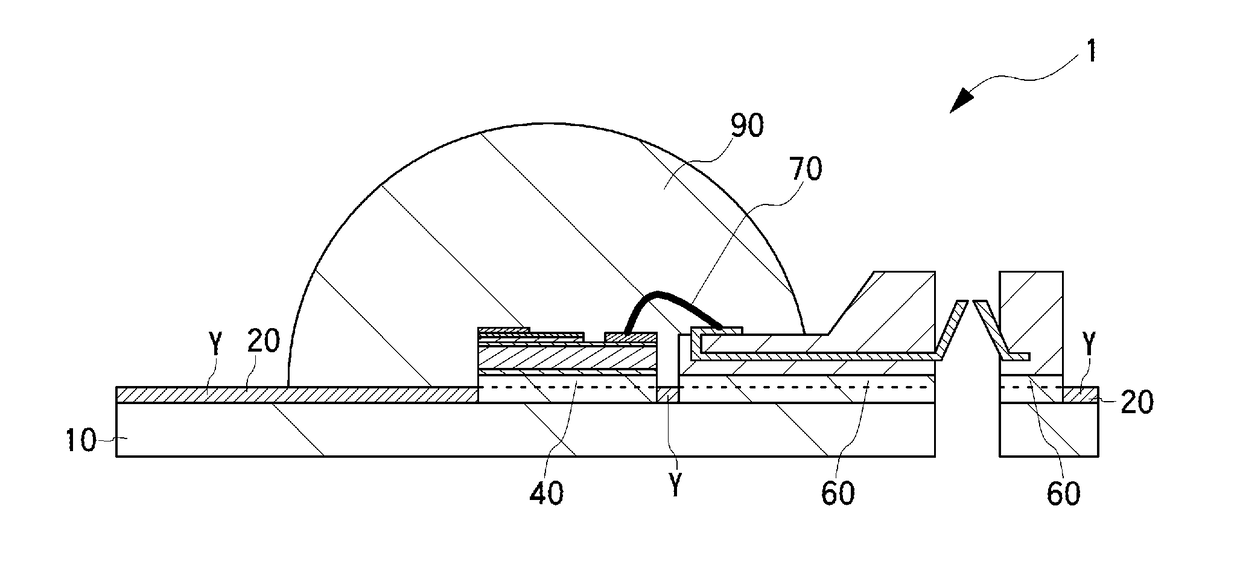
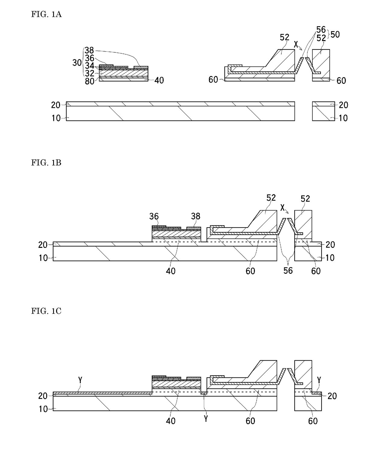
[0027]FIGS. 1A to 1F are schematic end surface views illustrating a method of manufacturing a semiconductor device 1 according to a first embodiment. FIG. 1A is a diagram illustrating disposing a substrate metal film 20, a first element metal film 40, and a second element metal film 60 (hereinafter may be collectively referred to as metal films 20, 40, and 60). FIG. 1B is a diagram illustrating bonding a first element 30 and a second element 50 to a substrate 10. FIG. 1C is a diagram illustrating a first oxidizing step. FIG. 1D is a diagram illustrating disposing a wiring 70. FIG. 1E is a diagram illustrating a second oxidizing step. FIG. 1F is a diagram illustrating disposing a sealing member 90. FIG. 2 is a schematic perspective view of the semiconductor device 1. FIG. 1A to FIG. 1F are end surface views taken along line A-A of FIG. 2, illustrating steps of manufacturing the semiconductor device 1.

[0028]As shown in FIG. 1A to FIG. 1F, ...

second embodiment

Method of Manufacturing Semiconductor Device 2

[0054]FIG. 3A to FIG. 3F are diagrams illustrating a method of manufacturing a semiconductor device 2 according to a second embodiment. FIG. 3A is an end surface view illustrating disposing a substrate metal film 20, a plurality of first element metal films 40, and a second element metal film 60. FIG. 3B is a top view illustrating bonding a plurality of first elements 30 and a second element 50 to a substrate 10. FIG. 3C is a top view illustrating disposing a wiring 70. FIG. 3D is an end surface view illustrating a first oxidizing step. FIG. 3E is an end surface view illustrating a second oxidizing step. FIG. 3F is an end surface view illustrating disposing a sealing member 90. FIG. 4 is a perspective view of the semiconductor device 2. For the simplicity of explanation, the sealing member 90 is not shown in FIG. 4. FIGS. 3A, 3D, 3E and 3F are end surface views taken in the line B-B of FIG. 4, illustrating steps of manufacturing the semi...


PUM


Abstract

A method of manufacturing a semiconductor device includes disposing a substrate metal film on an upper surface of a substrate made of a metal; disposing a first element metal film on a lower surface of a first element; disposing a second element metal film on a lower surface of a second element; bonding the first element and the second element to the substrate so that an upper surface of the substrate metal film is in contact with a lower surface of the first element metal film and a lower surface of the second element metal film; oxidizing at least a portion of a region of the upper surface of the substrate metal film other than regions in contact with the first element metal film and the second element metal film; and disposing a wiring electrically connecting the first element and the second element, across and above the region oxidized.

Description

CROSS-REFERENCE TO RELATED PATENT APPLICATION[0001]The present application claims priority under 35 U. S. C. § 119 to Japanese Patent Application No. 2016-217799, filed Nov. 8, 2016. The contents of this application are incorporated herein by reference in their entirety.BACKGROUNDTechnical Field[0002]The present disclosure relates to a method of manufacturing a semiconductor device.Description of Related Art[0003]Light emitting devices having a metal substrate and a plurality of light emitting elements have been proposed, for example, in Japanese Unexamined Patent Application Publication No. 2011-222574. The plurality of light emitting elements are mounted in a row on the metal substrate via an adhesive layer made of a silicone-based resin material, and are connected in series by using bonding wires as a wiring.SUMMARY[0004]In the light emitting devices as such described above, the adhesive layer is disposed between the light emitting elements and the metal substrate, which may redu...

Claims


Application Information

Patent Timeline
IPC IPC(8): H01L33/64H01L25/075H01L33/48H01L33/50H01L33/56H01L33/60H01L33/62
CPCH01L33/647H01L25/0753H01L33/486H01L33/502H01L33/56H01L33/60H01L33/62H01L2933/0041H01L2933/005H01L2933/0058H01L2933/0066H01L2933/0075H01L33/54H01L33/64H01L2933/0033H01L2224/48091H01L2224/48137H01L2924/00014
Inventor OKA, YUTAICHIKAWA, MASATSUGU
Owner NICHIA CORP
Why Eureka
Try Eureka