Voltage controlled clock synthesizer
- Summary
- Abstract
- Description
- Claims
- Application Information
AI Technical Summary
Benefits of technology
Problems solved by technology
Method used
Image


Examples
Embodiment Construction
)
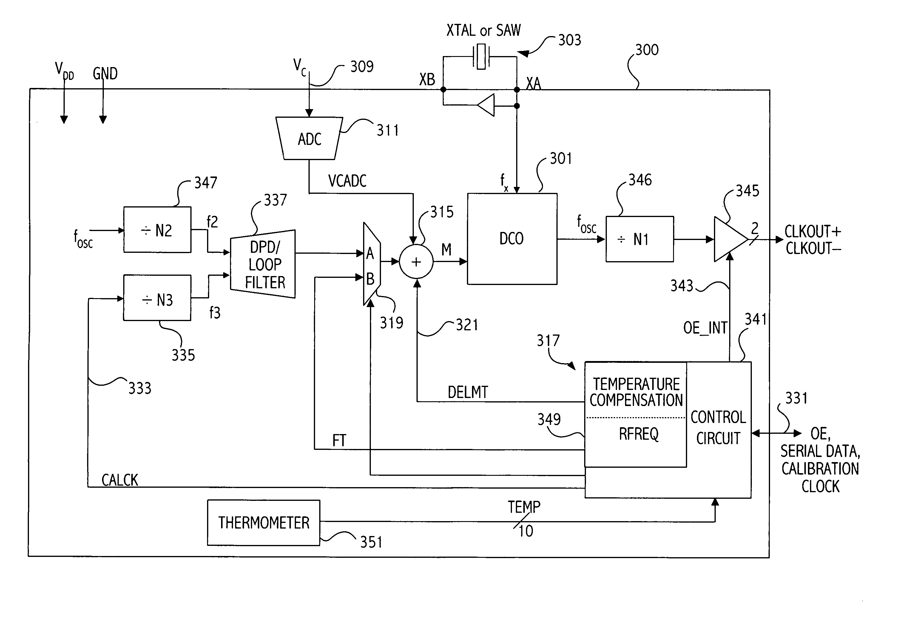
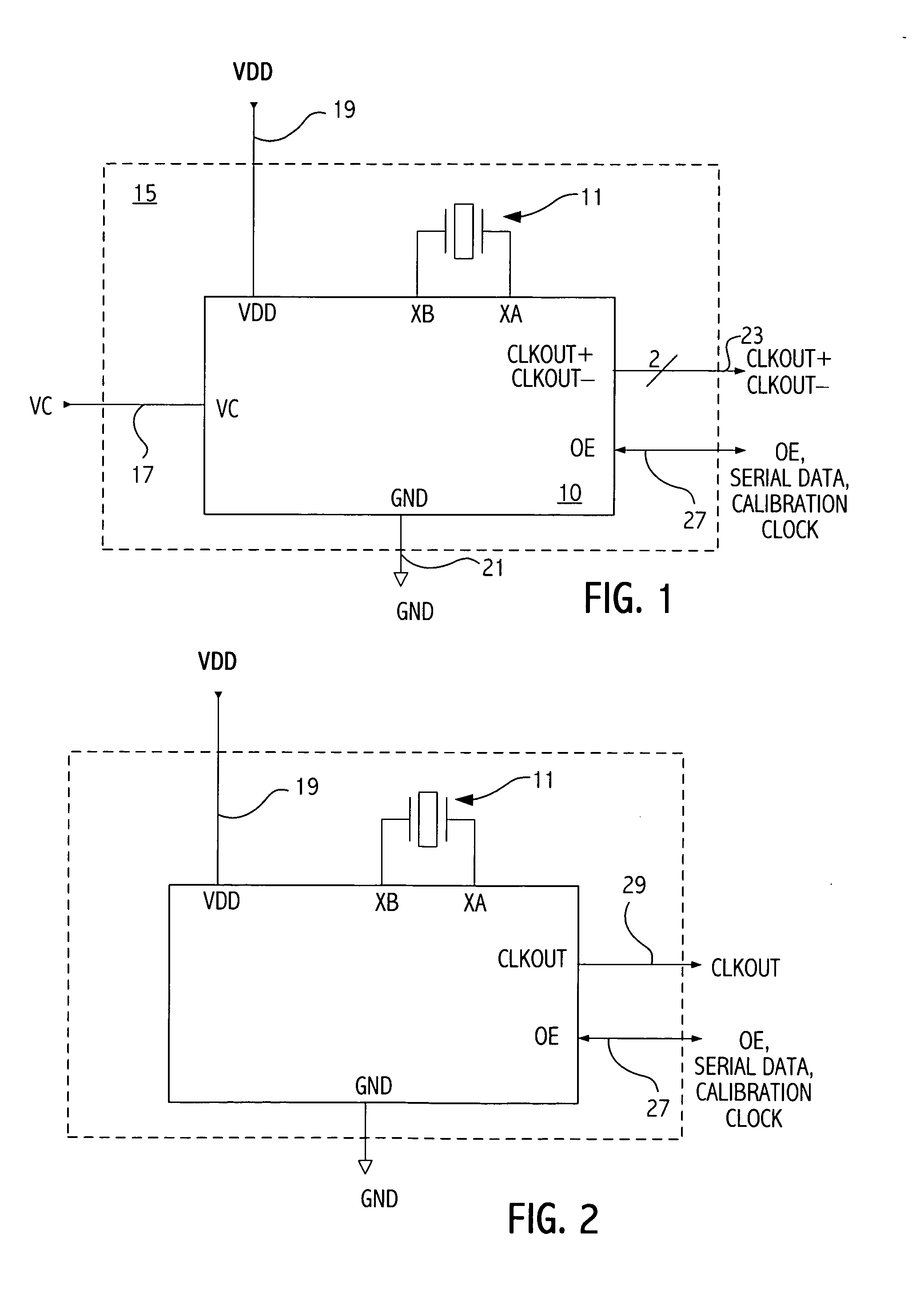
[0037] Referring to FIG. 1, a high level diagram shows a clock source device that includes an integrated circuit 10 coupled to a crystal 11. In one embodiment both the integrated circuit 10 and the crystal 11 are packaged in a standard ceramic package 15 that is typically utilized for packaging a voltage controlled crystal oscillator (VCXO). Note that another resonating device such as a surface acoustic wave (SAW) resonator may be utilized in place of crystal 11. In the illustrated embodiment, the package 15 includes standard input / output signals including a voltage control input 17, a power and ground input, 19 and 21 respectively, differential clock outputs and an output enable (OE) pin 27. FIG. 2 illustrates a four pin XO package implementation in which the control voltage input 17 is not utilized and the output clock 29 is single ended. A six pin XO package configuration may also be utilized in which the control voltage input on the package is not connected when the package 15 ...
PUM
 Abstract
Description
Claims
Application Information
 - R&D
- Intellectual Property
- Life Sciences
- Materials
- Tech Scout
- Unparalleled Data Quality
- Higher Quality Content
- 60% Fewer Hallucinations
Browse by: Latest US Patents, China's latest patents, Technical Efficacy Thesaurus, Application Domain, Technology Topic, Popular Technical Reports.
© 2025 PatSnap. All rights reserved.Legal|Privacy policy|Modern Slavery Act Transparency Statement|Sitemap|About US| Contact US: help@patsnap.com