Semiconductor device

Inactive Publication Date: 2015-11-19
MITSUBISHI ELECTRIC CORP
View PDF9 Cites 2 Cited by
  • Summary
  • Abstract
  • Description
  • Claims
  • Application Information

AI Technical Summary

Benefits of technology

The present invention aims to provide a semiconductor device that is smaller, has better heat dissipation, and allows for the mounting of semiconductor elements of different sizes. The device is designed to have easily connected electrodes, reducing the circuit area. The first and second semiconductor elements are not laminated to improve heat dissipation, and can be provided independently of each other without being restricted in their formation.

Problems solved by technology

Miniaturization of semiconductor devices has become a challenge, the semiconductor devices such as power modules including converter circuits that electrically connect vertical semiconductor devices in series in the same direction.
Thus, in a case where polarities of the chips (semiconductor elements) are connected in series in the same direction, relatively time-consuming wiring through electric wires such as a wire bonding and a metal pattern is required to electrically connect between an electrode formed on a front surface of one chip and an electrode formed on a back surface of the other chip because the chips to be connected have the polarities different from each other.
However, as with the techniques disclosed in Japanese Patent Application Laid-Open No. 2007-27432 and Japanese Patent Application Laid-Open No. 2008-244388, the semiconductor modules that laminate the plurality of vertical semiconductor devices in series connection have problems described below.
First of all, chips (upper side chips) mounted on chips (lower side chips) directly mounted on a supporting plate (substrate) have poor heat dissipation because the upper side chips are not in contact with the supporting plate, namely, the heat dissipating member.
Thus, the first problem is the poor heat dissipation.
Thus, the second problem is the unbalanced performances between the upper side chips and the lower side chips.

Method used


Image

  • Semiconductor device
  • Semiconductor device
  • Semiconductor device

Examples


first preferred embodiment

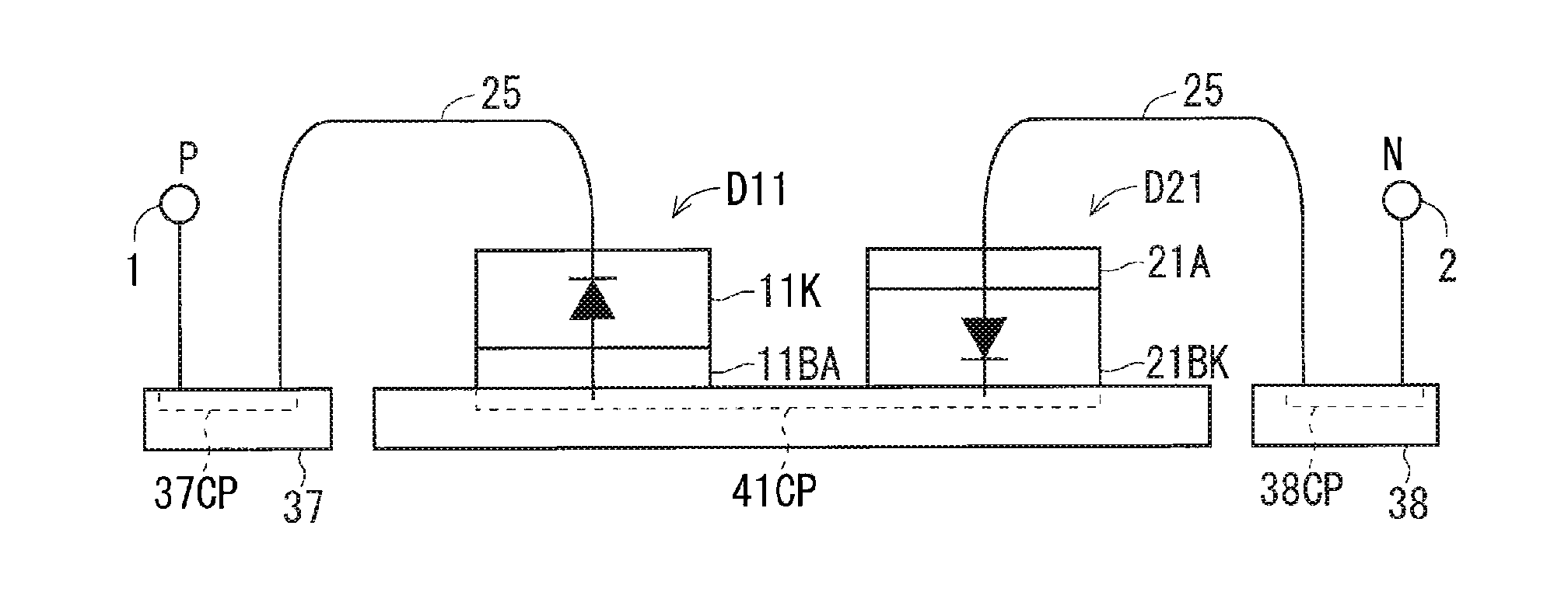
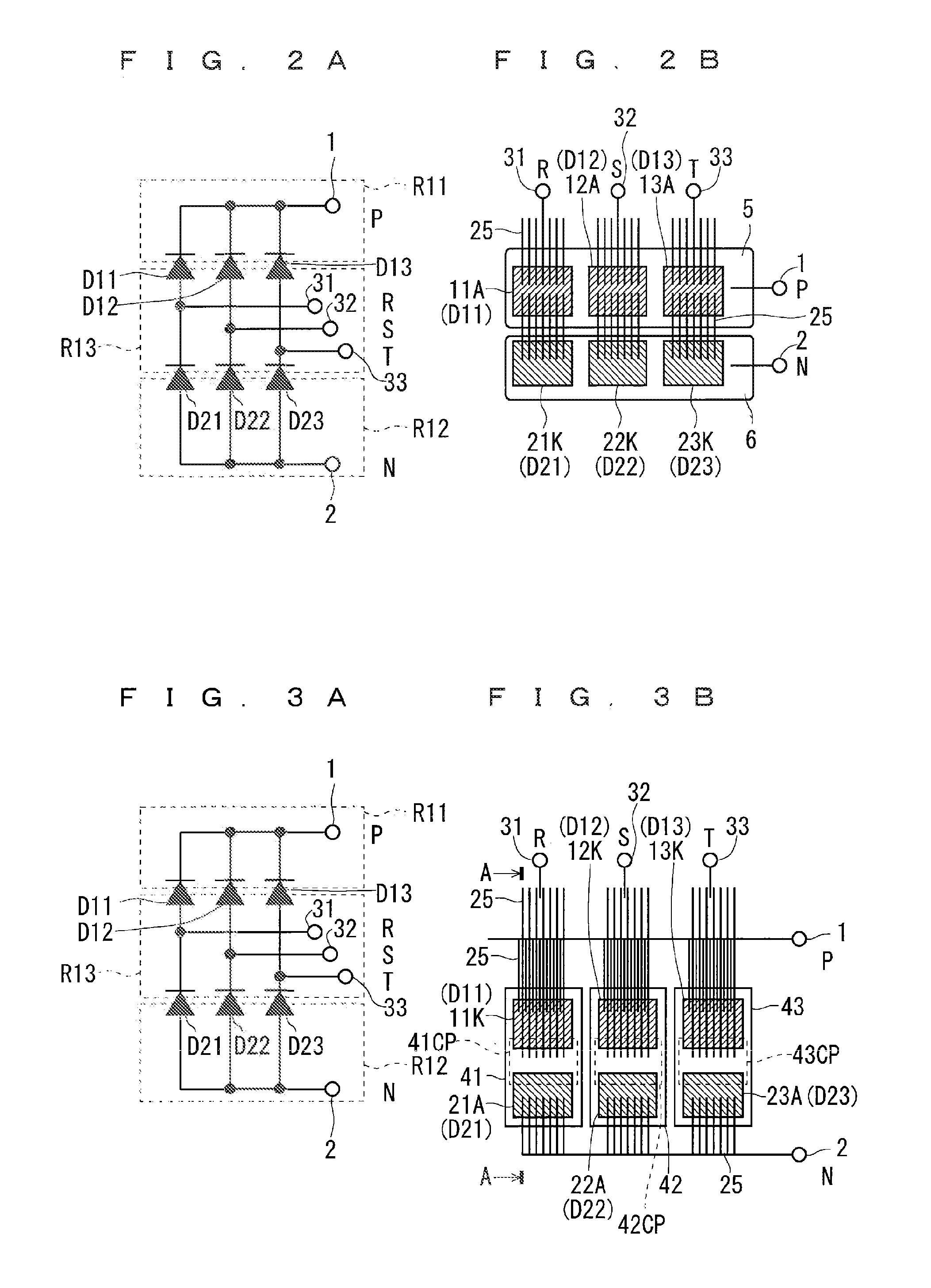
[0042]FIGS. 2A and 2B are explanatory diagrams showing a configuration of a power module including a converter circuit according to a first preferred embodiment of the present invention. Hereinafter, only the minimum number of circuit patterns required is shown because a product may have a configuration that wires directly connect chips (semiconductor elements) to an electrode portion in some cases.

[0043]As shown in FIG. 2A, the converter circuit is formed of diodes D11 to D13 (first semiconductor elements) and diodes D21 to D23 (second semiconductor elements). The diodes D11 to D13 (a plurality of first diodes) include anodes (one first electrode regions) and cathodes (the other first electrode regions). The diodes D21 to 23 (a plurality of second diodes) include anodes (one second electrode region) and cathodes (the other second electrode regions). Specifically, each of the cathodes of the diodes D11 to D13 is connected in common to a P terminal 1, the anodes of the diodes D11 to ...

second preferred embodiment

[0069]FIGS. 3A and 3B are explanatory diagrams showing a configuration of a power module including a converter circuit according to a second preferred embodiment of the present invention. Hereinafter, only the minimum number of circuit patterns required is shown because a product may have a configuration that wires directly connect chips to an electrode portion in some cases.

[0070]As shown in FIG. 3A, the converter circuit is formed of the diodes D11 to D13 and the diodes D21 to D23 similarly to the first preferred embodiment.

[0071]FIG. 3B shows a specific configuration for achieving the converter circuit shown in FIG. 3A. In other words, common patterns 41 to 43 (common circuit patterns (first and second circuit patterns)) are provided as circuit patterns for the converter circuit. The common patterns 41 to 43 are formed independently of one another on a substrate, which is not shown, for example. The circuit patterns for the P terminal 1, the N terminal 2, and the intermediate ter...

third preferred embodiment

[0092]FIGS. 5A, 5B, and 5C are explanatory diagrams showing a configuration of a power module including a step-down chopper circuit according to a third preferred embodiment of the present invention. Hereinafter, only the minimum number of circuit patterns required is shown because a product may have a configuration that wires directly connect chips to an electrode portion in some cases.

[0093]As shown in FIG. 5A, the step-down chopper circuit in the power module of the third preferred embodiment is formed of a combination (module portion defined by a dashed line) of an N-type IGBT 51 (first semiconductor element) and a diode D20 (second semiconductor element) as the main portion. The IGBT 51 includes an emitter (one first electrode region) and a collector (the other first electrode region). The diode D20 includes an anode (one second electrode region) and a cathode (the other second electrode region). Specifically, the collector of the IGBT 51 is connected to a P terminal 101, the e...


PUM


Abstract

A first diode having a front surface anode region is mounted on a P pattern, and a second diode having a front surface cathode region is mounted on an N pattern. At this time, the first diode and the second diode are formed such that a cathode region of a front surface anode region in a first vertical relationship and an anode region of a front surface cathode region in a second vertical relationship are always located as upper portions. The front surface anode region is electrically connected to the front surface cathode region with wires provided thereover.

Description

BACKGROUND OF THE INVENTION[0001]1. Field of the Invention[0002]The present invention relates to a semiconductor device such as a power module including a built-in circuit including a diode and more particularly to miniaturization of the device.[0003]2. Description of the Background Art[0004]Miniaturization of semiconductor devices has become a challenge, the semiconductor devices such as power modules including converter circuits that electrically connect vertical semiconductor devices in series in the same direction.[0005]In the semiconductor devices, chips such as a diode and a transistor forming semiconductor elements are mounted such that the same electrode surfaces have the same polarity. For example, in a case where a semiconductor device formed of a plurality of diodes is formed, anode electrodes are each disposed on front surfaces of all chips. Thus, in a case where polarities of the chips (semiconductor elements) are connected in series in the same direction, relatively ti...

Claims


Application Information

Patent Timeline
IPC IPC(8): H01L25/07H05K1/18H01L25/18
CPCH01L25/072H01L25/18H05K1/181H05K2201/10363H05K2201/10174H05K2201/10522H05K2201/1053H05K2201/10166H01L24/06H01L24/46H01L24/49H01L25/07H01L2224/48137H01L2224/49111H01L2224/49175H01L2224/73265H01L2924/19107H01L2924/13055H01L2924/13091H01L2924/00014H01L24/48H01L2224/05553H01L2224/0603H01L23/488H01L2924/00H01L2224/45099H01L2224/45015H01L2924/207H01L2224/05599
Inventor MASUDA, KOICHI
Owner MITSUBISHI ELECTRIC CORP
Why Eureka
Try Eureka