Method of protecting a mounting tape during laser singulation of a wafer

a technology of laser singulation and mounting tape, which is applied in the direction of semiconductor devices, semiconductor/solid-state device details, electrical equipment, etc., can solve the problems of limited range of available uv-resistant mounting tapes, limited use of uv dicing for mass production, and high cost of these uv-resistant mounting tapes. achieve the effect of cost-effectiveness

Active Publication Date: 2016-09-20
ASMPT SINGAPORE PTE LTD
View PDF10 Cites 0 Cited by
  • Summary
  • Abstract
  • Description
  • Claims
  • Application Information

AI Technical Summary

Benefits of technology

[0011]It is thus an object of the invention to seek to provide an effective and cost-effective method of cutting wafers using laser energy which avoids damaging the adhesive mounting tape on which the wafers are mounted.
[0013]According to a second aspect of the invention, there is provided a method of protecting a mounting tape supporting a semiconductor wafer from damage during laser singulation of the semiconductor wafer, comprising the steps of depositing a coating material onto a portion of the mounting tape adjacent to a perimeter of the semiconductor wafer to form a protective layer over the mounting tape prior to laser singulation.

Problems solved by technology

When UV laser radiation (such as by applying a laser beam having a wavelength of 355 nm) is used in the die singulation process, it is a challenge to combine the desirable UV-curing properties with sufficient resistance to UV laser radiation to avoid damage to the UV-resistant mounting tape during laser cutting.
Although some UV-resistant mounting tapes exist that combine these characteristics (being both UV curable and UV laser-resistant), the range of available UV-resistant mounting tapes is very limited and the costs of these UV-resistant mounting tapes are very high, thereby limiting the use of UV dicing for the purpose of mass production.
As a result, semiconductor manufacturers resort to the use of these exotic tapes only for applications that can tolerate the additional cost of the UV-resistant mounting tape.
Alternatively, solutions based on green or infrared laser have been developed, but they are inferior when compared to a UV laser singulation solution, since they result in larger kerf-widths, more recast and larger burrs.
For UV laser cutting applications, this requires expensive custom-made mounting tapes.
This is difficult to achieve in practice, and even if feasible, would place additional requirements on the accuracy and performance of the singulation machine.
Hence, at present, there is a severe limitation in the choice of suitable adhesive mounting tapes to support UV laser wafer singulation applications.
This means that an end-user has to adopt newer and much more expensive UV-resistant mounting tapes for this purpose.
In general, this becomes a very significant barrier for an end-user to consider adopting a UV laser singulation process, even though the singulation results might be superior and more cost-effective.
Even if the end-user decides to use such novel UV-curable and UV laser-resistant mounting tapes, any unintended cuts in the mounting tape is considered undesirable, since the UV-resistant mounting tape may still be punctured and lead to the loss of wafers, either in the singulation machine itself or during subsequent die-picking steps.
These risks are further increased when high-power and multi-pass UV laser singulation processes are used.
Furthermore, in laser-singulation applications where multiple cutting lines are cut simultaneously, it is extremely difficult to avoid cutting into the mounting tape.

Method used


Image

  • Method of protecting a mounting tape during laser singulation of a wafer
  • Method of protecting a mounting tape during laser singulation of a wafer
  • Method of protecting a mounting tape during laser singulation of a wafer

Examples


Embodiment Construction

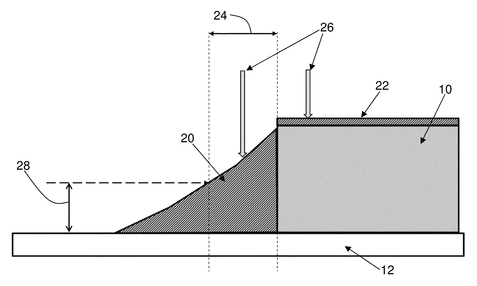
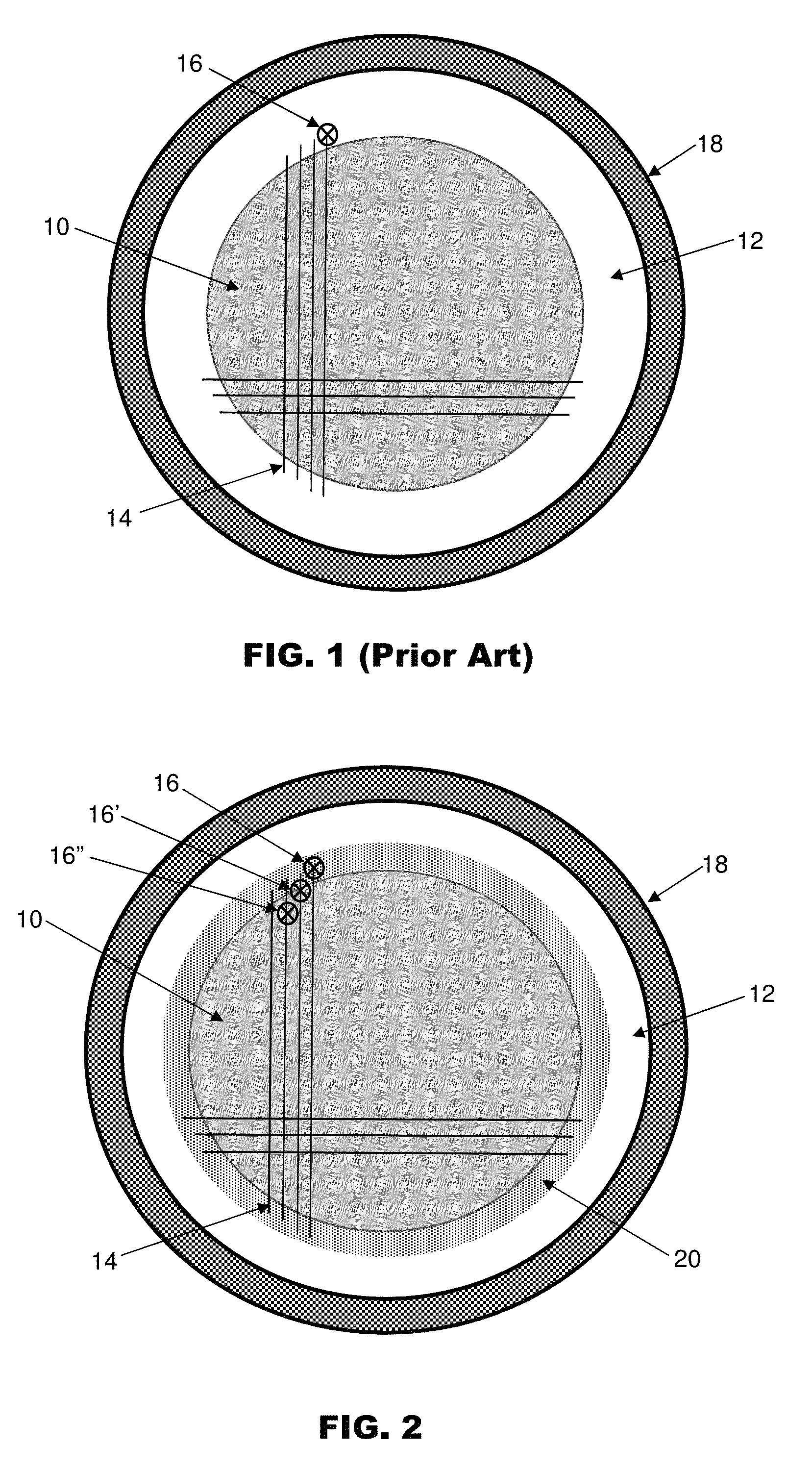
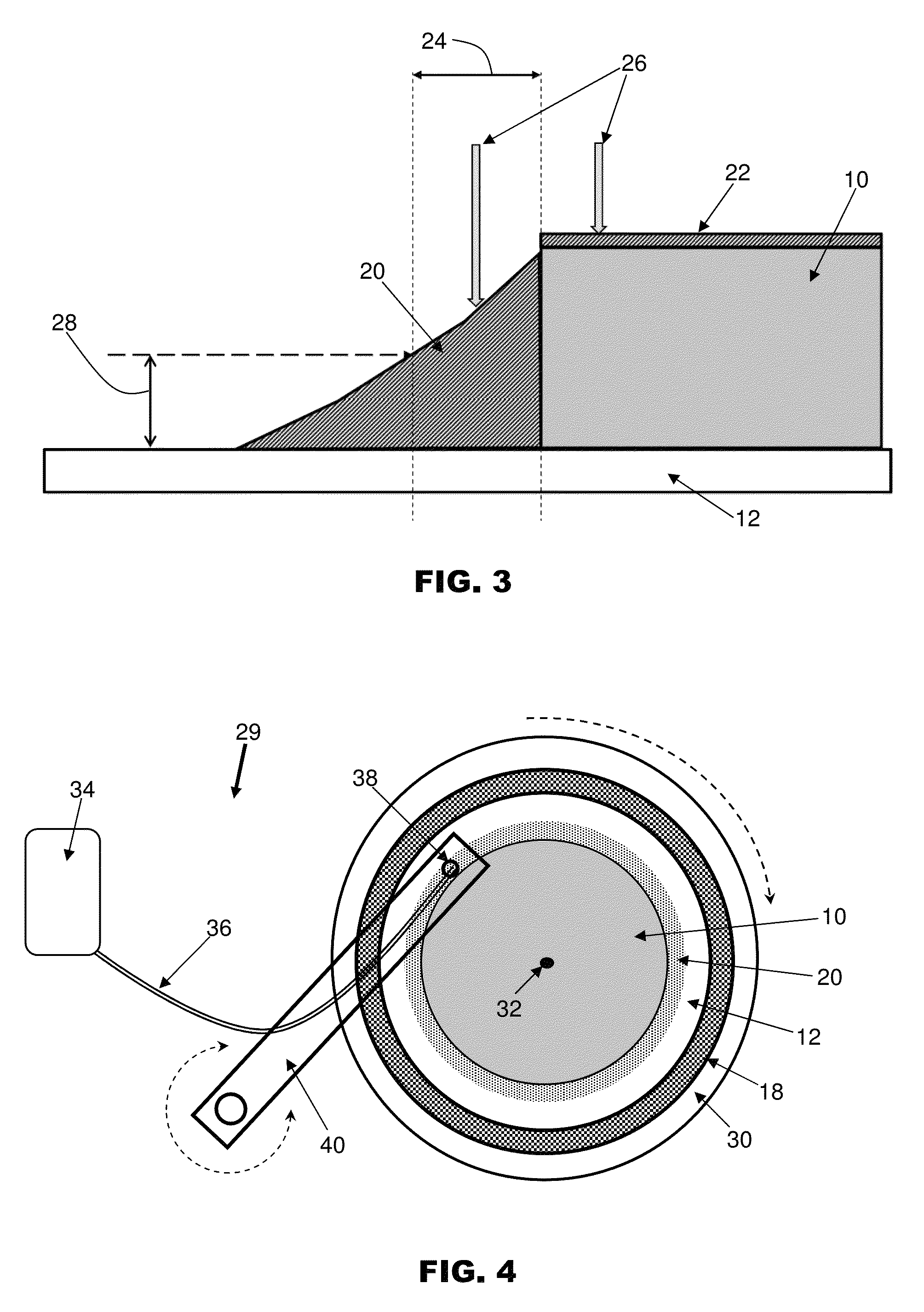
[0020]FIG. 2 illustrates a protective layer 20 coated on the adhesive mounting tape 12 adjacent to a perimeter of the semiconductor wafer 10 for protecting the adhesive mounting tape 12 during laser singulation. Laser singulation may be performed by dicing or grooving. The laser beam used has an ultraviolet (“UV”) wavelength. Additional laser beams 16′, 16″ may also be used during singulation for cutting multiple points simultaneously.

[0021]The coating material used to form the protective layer 20 is selected to be in viscous form when deposited but hardens when set, and is also easily removable after use. The protective layer 20 preferably surrounds a whole perimeter of the semiconductor wafer 10 to protect the adhesive mounting tape 12 against harmful incident laser beams such as UV laser radiation that would normally damage the adhesive mounting tape 12 when the laser beam 16 moves beyond the boundary of the edge of the semiconductor wafer 10. By forming the protective layer 20, ...


PUM


Abstract

A method of singulating a semiconductor wafer with laser energy while the semiconductor wafer is supported on a mounting tape during singulation comprises the step of depositing a coating material onto a portion of the mounting tape adjacent to a perimeter of the semiconductor wafer to form a protective layer over the mounting tape. The semiconductor wafer is then cut with a laser beam such that the laser beam at least partially impinges upon the protective layer during cutting of the semiconductor wafer. After singulation of the semiconductor wafer, the protective layer is removed from the mounting tape.

Description

FIELD OF THE INVENTION[0001]The invention relates to semiconductor wafer singulation, and in particular, to semiconductor wafer singulation conducted on a wafer that is mounted onto an adhesive tape.BACKGROUND AND PRIOR ART[0002]Laser cutting of semiconductor wafers comprising a plurality of semiconductor dice is commonly used as an efficient and accurate die-singulation process. Such laser cutting may be conducted by cutting completely through the wafer in a process called dicing or by forming grooves in the wafer in a process called grooving. The wafer that needs to be singulated is mounted onto a special mounting tape, which may be in the form of a polymer adhesive mounting tape that holds the individual dice in place during the singulation process. Additionally, the singulated dice are also held in place after laser singulation when the wafer and the tape are transferred to the next tool for further processing. There are many different types of adhesive mounting tape available d...

Claims


Application Information

Patent Timeline
Patent Type & Authority Patents(United States)
IPC IPC(8): H01L21/78H01L21/428H01L23/00
CPCH01L21/78H01L21/428H01L24/03H01L2224/03009H01L21/6836H01L2221/68327H01L2221/68381
Inventor ERNST, FRANKEVERTSEN, ROGIERPIETERS, RAPHMULLER, MARKKNIPPELS, GUIDO
Owner ASMPT SINGAPORE PTE LTD
Why Eureka
Try Eureka