Stacked photonic chip coupler for SOI chip-fiber coupling

a technology of soi chip and photonic chip, applied in the field of optical transmission system, can solve the problems of large optical loss, significant affecting the efficiency of the photonic chip, and optical loss

Active Publication Date: 2016-09-06
HUAWEI TECH CO LTD
View PDF13 Cites 28 Cited by
  • Summary
  • Abstract
  • Description
  • Claims
  • Application Information

AI Technical Summary

Problems solved by technology

However, conventional edge coupling contributes to large optical loss (e.g., fiber-to-SOI chip), which significantly affects the efficiency of the photonic chip.
This optical loss is often attributed to a large mismatch between the optical fiber and the silicon-on-insulator (SOI) waveguide mode (e.g., 10 microns versus 0.5 microns) and because of optical leakage due to a high index of refraction substrate.

Method used


Image

  • Stacked photonic chip coupler for SOI chip-fiber coupling
  • Stacked photonic chip coupler for SOI chip-fiber coupling
  • Stacked photonic chip coupler for SOI chip-fiber coupling

Examples


Embodiment Construction

[0014]The making and using of the presently preferred embodiments are discussed in detail below. It should be appreciated, however, that the present invention provides many applicable inventive concepts that can be embodied in a wide variety of specific contexts. The specific embodiments discussed are merely illustrative of specific ways to make and use the invention, and do not limit the scope of the invention.

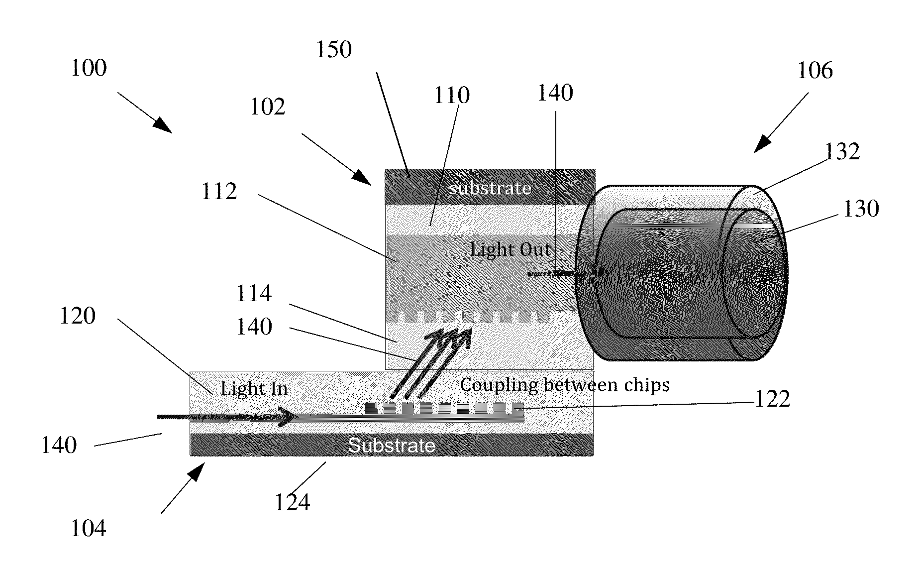
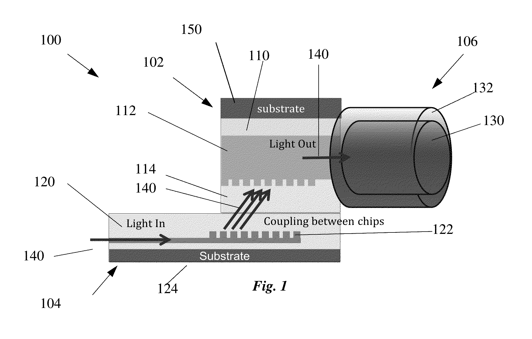
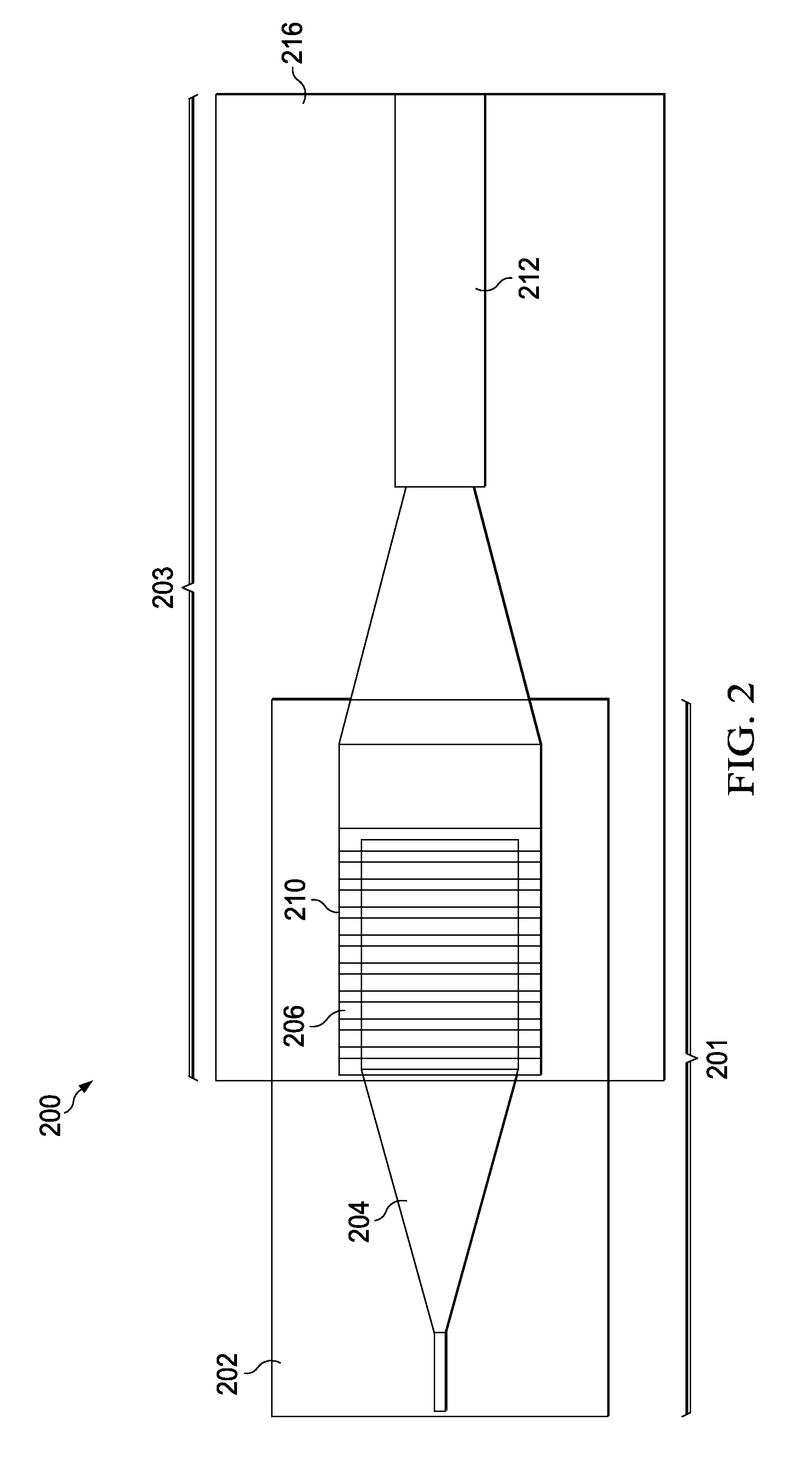
[0015]Silicon nanophotonic circuits exhibit highly compact and high level of function integration due to its high index contrast based on a SOI platform. The waveguide cross-section of silicon nanophotonic circuits is within a sub-micron scale. To implement the silicon chip within data optical transmission networks, such circuits must be connected with optical fibers (or other optical transmission means) which usually have a 10 micron mode field dimension (MFD). Such a mismatch between the silicon waveguide and the optical fiber leads to significant loss at this interface. It...


PUM


Abstract

Embodiments are provided for an optical coupler created by bonded photonic chip coupler for Silicon-on-Insulator (SOI) chip-fiber coupling. System and apparatus embodiments for a bonded photonic chip coupler for SOI chip-fiber coupling provide for reduced mismatch between fiber and chip, increased coupling efficiency, and lower photonics device insertion loss. In an embodiment, an optical coupler for coupling a photonics chip to an optical fiber includes a photonic chip comprising a nano-sized photonic waveguide, photonic optical diffraction surface grating, and a first cladding covering the photonic waveguide and the photonic grating; and an optical coupling chip comprising a micron-sized coupling waveguide and a coupling optical diffraction surface grating embedded in a first coupling cladding and on a second coupling cladding, wherein the first coupling cladding is connected to the first cladding, wherein the optical coupling chip is configured to couple to light transmitted between the photonic chip and an optical fiber.

Description

TECHNICAL FIELD[0001]The present invention relates to an optical transmission system, and, in particular embodiments, to a systems and apparatuses for photonic chip to fiber coupling.BACKGROUND[0002]Edge coupling is a conventional approach to realize fiber-to-photonic chip coupling since it can work in a broad range of wavelengths and it is compatible with mature package technology for larger photonic chips, such as, for example, silica-on-silicon technology. However, conventional edge coupling contributes to large optical loss (e.g., fiber-to-SOI chip), which significantly affects the efficiency of the photonic chip. This optical loss is often attributed to a large mismatch between the optical fiber and the silicon-on-insulator (SOI) waveguide mode (e.g., 10 microns versus 0.5 microns) and because of optical leakage due to a high index of refraction substrate.SUMMARY[0003]In accordance with an embodiment, an optical coupler for coupling a photonics chip to an optical fiber includes...

Claims


Application Information

Patent Timeline
Patent Type & Authority Patents(United States)
IPC IPC(8): G02B6/12H01L31/167G02B6/34
CPCG02B6/34H01L31/167G02B6/1223G02B6/124G02B6/305G02B6/356G02B2006/12061G02B2006/12164
Inventor JIANG, JIA
Owner HUAWEI TECH CO LTD
Why Eureka
Try Eureka