
Nanowire or 2D material strips interconnects in an integrated circuit cell

a technology of integrated circuit cells and nanowires, which is applied in the field of integrated circuit devices, cell libraries, cell architectures and electronic design automation tools for integrated circuit devices, can solve the problems of complex reconfiguration of fins or other structures, labor-intensive process for cell design, etc., and achieve different performance characteristics of cells and gradations of drive power

Active Publication Date: 2016-06-07
SYNOPSYS INC
View PDF33 Cites 9 Cited by
  • Summary
  • Abstract
  • Description
  • Claims
  • Application Information

AI Technical Summary

Benefits of technology

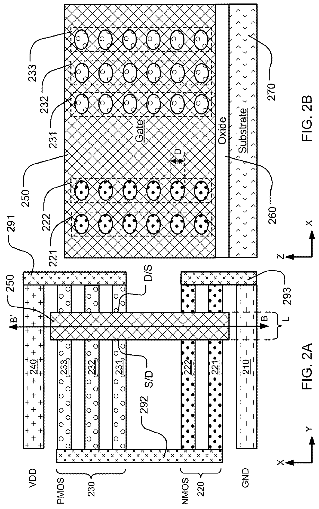
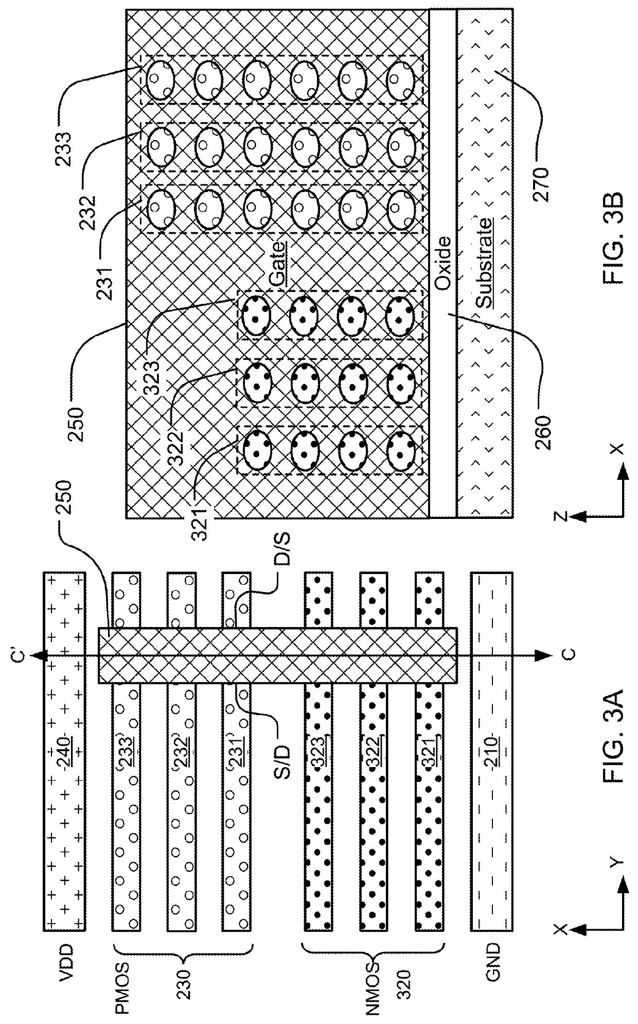
[0016]A method for designing a circuit based on nanowires or on 2D material strips, a resulting cell architecture and an integrated circuit design tool utilizing the cell architecture, are described. Specifications of a particular cell in a computer readable description language can include transistors and interconnects implemented utilizing nanowires or 2D material strips. Thus, a computer implemented cell can comprise a specification of a circuit including a first transistor and a second transistor. The first transistor can include a first set of nanowires or 2D material strips arranged in parallel to form a channel structure, and a gate conductor disposed across the first set of nanowires or 2D material strips. The second transistor can include a second set of nanowires or 2D material strips arranged in parallel to form a channel structure, and a gate conductor disposed across the first set of nanowires or 2D material strips. The number of nanowires or of 2D material strips in the first set can be different from the number of nanowires or of 2D material strips in the second set, so that the drive power of the individual transistors, and other circuit performance characteristics, can be set with finer granularity.
[0018]A cell library is described taking advantage of this granularity, which can include a set of cells that implements a common circuit, such as an inverter, a NAND gate or other common logic cell. The cells implementing the common circuit can differ in the number of parallel nanowires used in the implementation of a particular transistor in the common circuit. Also, the cells in the set of cells can differ in the number of parallel nanowires used in the implementation of a particular interconnect in the common circuit. These variations in the number of parallel nanowires can provide for finer gradations in drive power or other characteristics of the transistors, and correspondingly different performance characteristics for the cell.

Problems solved by technology

The procedure of designing cells to be specified in a cell library is often a labor-intensive process, requiring highly skilled designers to manually design and refine the designs of the cells.
To fine tune finFET type circuits, complex reconfiguration of the fins or other structures may be required.

Method used


Image

  • Nanowire or 2D material strips interconnects in an integrated circuit cell
  • Nanowire or 2D material strips interconnects in an integrated circuit cell
  • Nanowire or 2D material strips interconnects in an integrated circuit cell

Examples


Embodiment Construction

[0069]A detailed description of embodiments of the present invention is provided with reference to the Figures. The following description will typically be with reference to specific structural embodiments and methods. It is to be understood that there is no intention to limit the invention to the specifically disclosed embodiments and methods but that the invention may be practiced using other features, elements, methods and embodiments. Preferred embodiments are described to illustrate the present invention, not to limit its scope, which is defined by the claims. Those of ordinary skill in the art will recognize a variety of equivalent variations on the description that follows. Like elements in various embodiments are commonly referred to with like reference numerals.

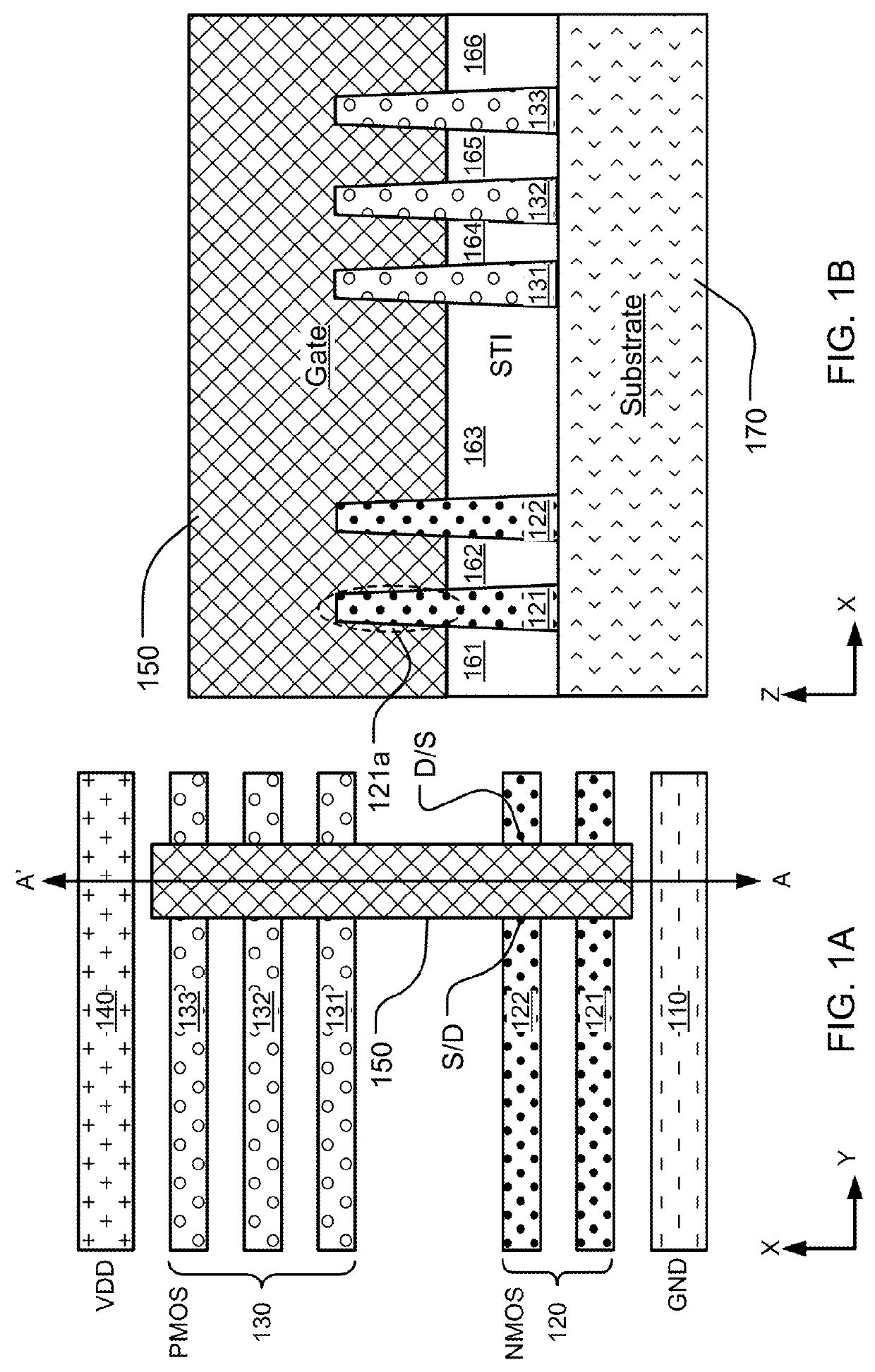
[0070]FIGS. 1A and 1B illustrate complementary finFET blocks in which finFET transistors can be arranged to implement cells. The cells can be in a flexible finFET cell library. FIG. 1A shows a top view of a finFET st...


PUM


Abstract

An integrated circuit design tool includes a cell library. The cell library includes entries for a plurality of cells, entries in the cell library including specifications of particular cells in a computer executable language. At least one entry in the cell library can comprise a specification of physical structures and timing parameters of a circuit including a first transistor, a second transistor, and an interconnect connecting a terminal of the first transistor to a terminal of the second transistor, the interconnect comprising one or more nanowires or 2D material strips arranged in parallel. An integrated circuit including the circuit is described.

Description

BACKGROUND[0001]1. Field of the Invention[0002]The present invention relates to integrated circuit devices, cell libraries, cell architectures and electronic design automation tools for integrated circuit devices.[0003]2. Description of Related Art[0004]In the design of integrated circuits, standard cell libraries are often utilized. The process of designing the cells specified by entries in the cell libraries can be intensive, where trade-offs among variables such as the size of the cells, the drive power of the cells, the speed of the cells and so on, are made by adjusting the materials, geometry and size of the components of the cell. The procedure of designing cells to be specified in a cell library is often a labor-intensive process, requiring highly skilled designers to manually design and refine the designs of the cells.[0005]The development of finFETs has provided some additional flexibility for designers which can be applied in the efficient design of variations of specific...

Claims


Application Information

Patent Timeline
Patent Type & Authority Patents(United States)
IPC IPC(8): G06F17/50
CPCG06F17/5072G06F17/5077G06F30/392G06F30/394H01L21/76895H01L21/823807H01L21/823885H01L27/092H01L27/1203H01L29/0676H01L29/42392H01L29/78642H01L29/78696H01L2221/1094H01L23/5226H01L23/528H01L23/53271H01L27/0207H01L29/0649H01L29/0673H01L29/1033
Inventor MOROZ, VICTORKAWA, JAMIL
Owner SYNOPSYS INC
Learn More