Semiconductor device

a technology of semiconductor devices and semiconductors, applied in semiconductor devices, semiconductor/solid-state device details, electrical apparatus, etc., can solve the problems of unintentional cutting or separation of wires, reducing manufacturing efficiency, and comparatively thin wires, so as to enhance manufacturing efficiency and improve manufacturing efficiency

Active Publication Date: 2016-05-31
ROHM CO LTD
View PDF4 Cites 2 Cited by
  • Summary
  • Abstract
  • Description
  • Claims
  • Application Information

AI Technical Summary

Benefits of technology

[0006]The present invention has been proposed under the above circumstances, and an object of the present invention is to provide a semiconductor device that can enhance manufacturing efficiency and enables the semiconductor element to be more reliably joined to the conduction connection member. Also, another object of the present invention is to provide a semiconductor device that can enhance manufacturing efficiency and enables the semiconductor element to be more reliably joined to the heat dissipation member.

Problems solved by technology

This is thus an impediment to improving the manufacturing efficiency of the semiconductor device.
Also, the wires are comparatively thin, and thus could possibly be unintentionally cut or separate during the manufacturing process of the semiconductor device or use of the semiconductor device.

Method used


Image

  • Semiconductor device
  • Semiconductor device
  • Semiconductor device

Examples


first embodiment

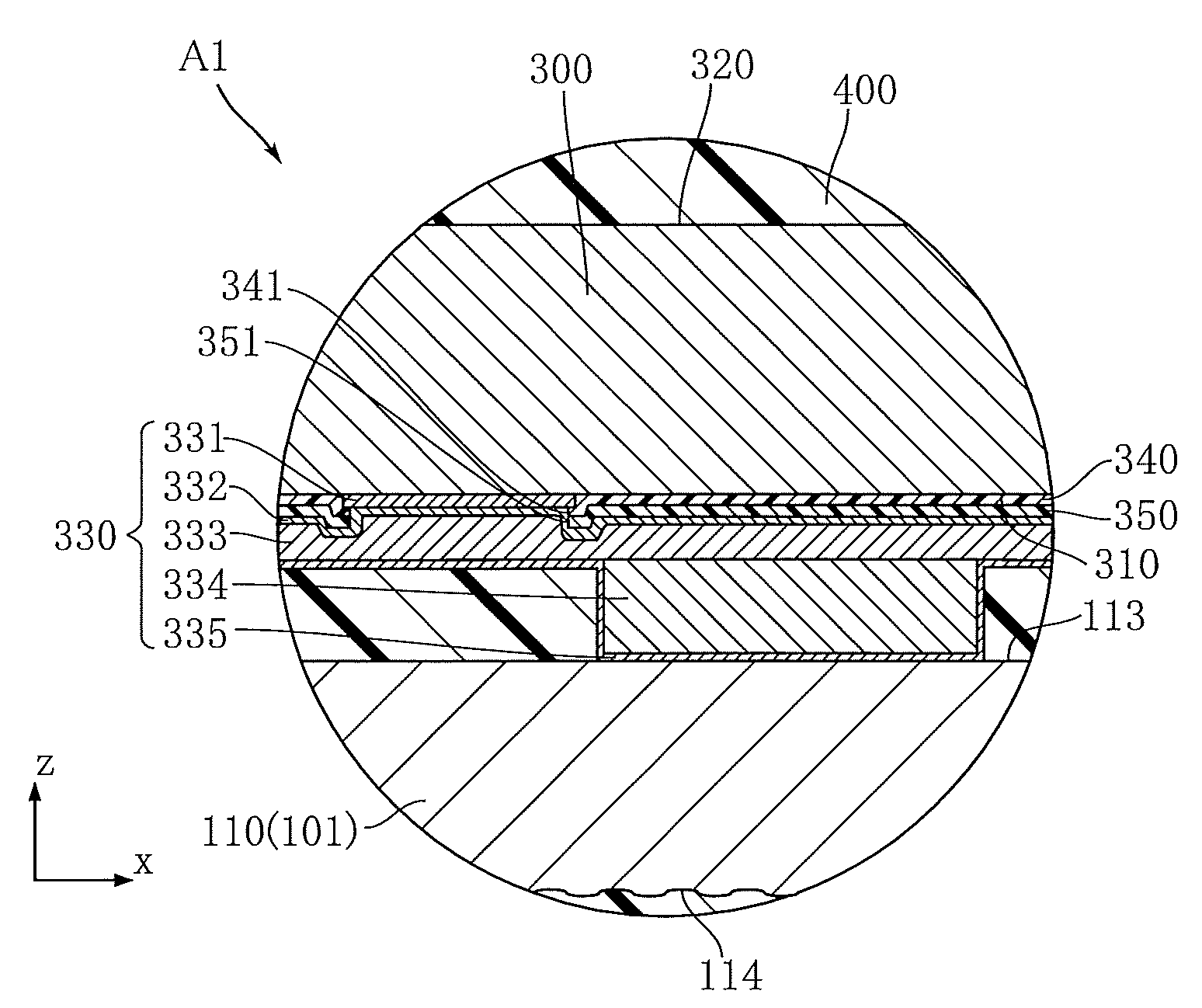
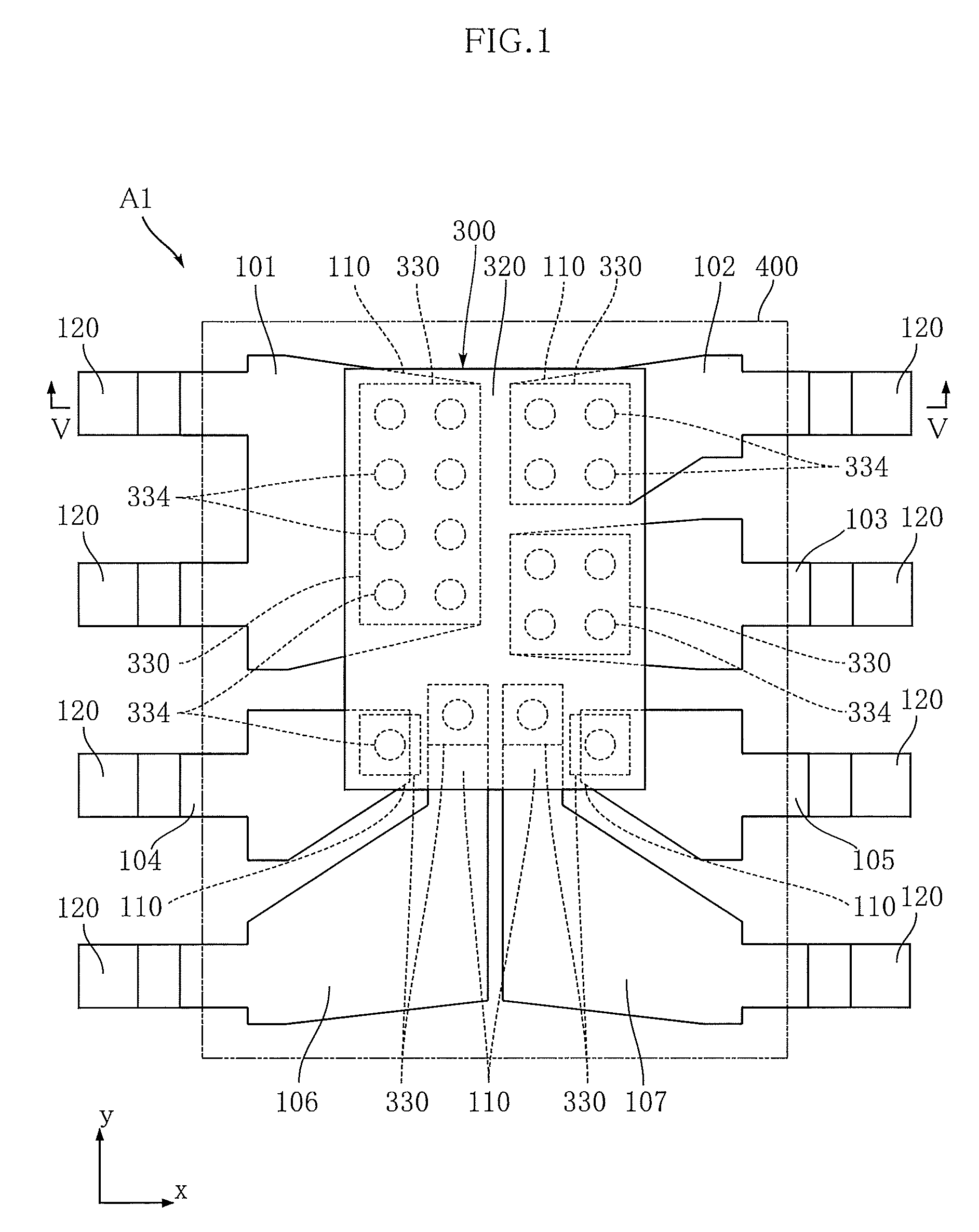
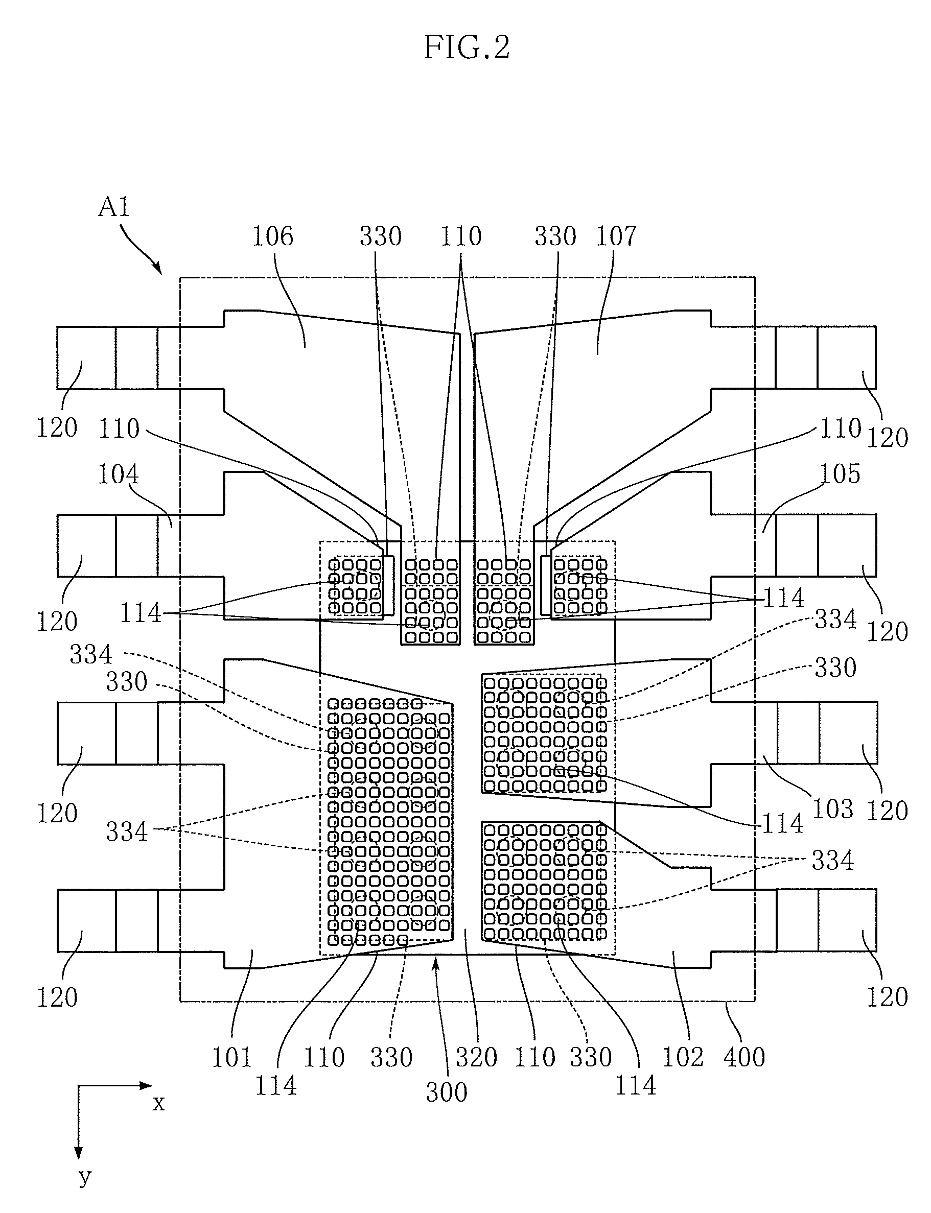
[0135]FIGS. 1 to 6 show a semiconductor device that is based on the present invention. A semiconductor device A1 of the present embodiment is provided with leads 101 to 107, a semiconductor element 300, and a sealing resin 400.

[0136]FIG. 1 is a plan view showing the semiconductor device A1. FIG. 2 is a bottom view showing the semiconductor device A1. FIG. 3 is a front view showing the semiconductor device A1. FIG. 4 is a side view showing the semiconductor device A1. FIG. 5 is a cross-sectional view along a line V-V in FIG. 1. FIG. 6 is an enlarged cross-sectional view showing a main section of the semiconductor device A1.

[0137]The leads 101 to 107 are examples of a conduction supporting member as referred to in the present invention. The leads 101 to 107 constitute conduction paths between the semiconductor element 300 and outside the semiconductor device A1, and support the semiconductor element 300. The leads 101 to 107 are made of a metal, and are preferably made of either Cu or...

second embodiment

[0172]FIGS. 15 to 20 show a semiconductor device that is based on the present invention. A semiconductor device A2 of the present embodiment is provided with leads 101 to 107, a semiconductor element 300, and a sealing resin 400.

[0173]FIG. 15 is a plan view showing the semiconductor device A2. FIG. 16 is a bottom view showing the semiconductor device A2. FIG. 17 is a front view showing the semiconductor device A2. FIG. 18 is a side view showing the semiconductor device A2. FIG. 19 is a cross-sectional view along a line XIX-XIX in FIG. 15. FIG. 20 is an enlarged cross-sectional view showing a main section of the semiconductor device A2.

[0174]The leads 101 to 107 are examples of a conduction supporting member as referred to in the present invention. The leads 101 to 107 constitute conduction paths between the semiconductor element 300 and outside the semiconductor device A2, and support the semiconductor element 300. The leads 101 to 107 are made of a metal, and are preferably made of...

third embodiment

[0197]FIGS. 25 to 30 show a semiconductor device that is based on the present invention. A semiconductor device A3 of the present embodiment is provided with leads 101 to 107, a heat dissipation member 200, a semiconductor element 300, and a sealing resin 400.

[0198]FIG. 25 is a plan view showing the semiconductor device A3. FIG. 26 is a bottom view showing the semiconductor device A3. FIG. 27 is a front view showing the semiconductor device A3. FIG. 28 is a side view showing the semiconductor device A3. FIG. 29 is a cross-sectional view along a line XXIX-XXIX in FIG. 25. FIG. 30 is an enlarged cross-sectional view showing a main section of the semiconductor device A3.

[0199]The leads 101 to 107 are examples of a conduction supporting member as referred to in the present invention. The leads 101 to 107 constitute conduction paths between the semiconductor element 300 and outside the semiconductor device A3, and support the semiconductor element 300. The leads 101 to 107 are made of a ...


PUM


Abstract

A semiconductor device has a semiconductor element provided with a functional surface on which a functional circuit is formed and with a back surface facing in the opposite direction to the functional surface, while also having a lead supporting the semiconductor element and electrically connected to the semiconductor element, and a resin package covering at least a portion of the semiconductor element and the lead. The semiconductor element has a functional surface side electrode formed on the functional surface and equipped with a functional surface side raised part that projects in the direction in which the functional surface faces. The functional surface side raised part of the functional surface side electrode is joined to the lead by solid state bonding.

Description

BACKGROUND OF THE INVENTION[0001]1. Field of the Invention[0002]The present invention relates to a semiconductor device.[0003]2. Description of Related Art[0004]In a semiconductor device having a built-in semiconductor element, a conduction supporting member that constitutes a conduction path to the semiconductor device and supports the semiconductor element is used. In such a semiconductor device, a lead made of a metal is used as the conduction supporting member. A plurality of wires made of Au or the like are used as means for electrically connecting the semiconductor element to the lead. Known documents relating to semiconductor devices include JP-A-2014-7363, for example.[0005]In the manufacturing process of the semiconductor device, a process for bonding the plurality of wires is executed. This bonding process is performed sequentially on the plurality of wires, and cannot be executed collectively on the plurality of wires. This is thus an impediment to improving the manufactu...

Claims


Application Information

Patent Timeline
Patent Type & Authority Patents(United States)
IPC IPC(8): H01L23/495H01L23/433H01L23/482H01L23/29H01L23/52H01L23/00H01L23/31H01L23/525
CPCH01L24/33H01L23/291H01L23/3107H01L23/3142H01L23/3171H01L23/4334H01L23/4822H01L23/49548H01L23/49551H01L23/49572H01L24/02H01L24/05H01L24/13H01L24/17H01L24/75H01L24/81H01L24/83H01L2224/13582H01L2224/13664H01L2224/13655H01L2224/75301H01L2924/00012H01L2224/753H01L2224/83201H01L2924/00014H01L2224/29155H01L2224/29164H01L2224/29124H01L2224/29147H01L2224/29166H01L2224/29144H01L2224/05124H01L2224/13016H01L2224/05572H01L2224/11825H01L2224/0346H01L2224/05147H01L2924/186H01L2924/0665H01L2924/17747H01L2924/181H01L2924/182H01L23/525H01L24/03H01L24/11H01L24/16H01L24/73H01L2224/024H01L2224/0239H01L2224/02311H01L2224/02331H01L2224/0345H01L2224/03452H01L2224/03462H01L2224/05008H01L2224/05073H01L2224/05082H01L2224/05083H01L2224/05084H01L2224/05155H01L2224/05181H01L2224/05548H01L2224/05567H01L2224/05582H01L2224/05624H01L2224/05644H01L2224/05647H01L2224/05655H01L2224/05664H01L2224/05666H01L2224/1145H01L2224/1146H01L2224/1147H01L2224/1161H01L2224/13008H01L2224/13011H01L2224/13017H01L2224/13019H01L2224/13024H01L2224/13147H01L2224/13624H01L2224/13644H01L2224/13647H01L2224/13666H01L2224/16014H01L2224/16245H01L2224/16258H01L2224/17107H01L2224/29082H01L2224/32245H01L2224/73253H01L2224/75981H01L2224/8146H01L2224/8183H01L2224/81191H01L2224/81192H01L2224/81201H01L2224/81439H01L2224/81444H01L2224/81447H01L2224/81455H01L2224/81464H01L2224/81466H01L2224/8346H01L2224/8383H01L2224/83191H01L2224/83439H01L2224/83444H01L2224/83447H01L2224/83455H01L2224/83464H01L2224/83466H01L2224/92225H01L2924/01013H01L2924/01022H01L2924/01029H01L2924/01073H01L2924/01074H01L2924/05042H01L2924/07025H01L2924/17724H01L2224/05166H01L2924/01028H01L2224/48137H01L23/293H01L23/3675H01L24/29H01L2224/29008H01L23/3114H01L23/49503H01L23/49527H01L23/49568H01L2224/0401H01L2224/05583H01L2224/05681H01L2224/05684H01L2224/13561
Inventor FUJII, KENJIKASUYA, YASUMASAYAMAGAMI, MAMORUKINOSHITA, NAOKIHAGA, MOTOHARU
Owner ROHM CO LTD
Why Eureka
Try Eureka