
Niobium based superconducting radio frequency(SCRF) cavities comprising niobium components joined by laser welding, method and apparatus for manufacturing such cavities

Inactive Publication Date: 2016-05-31
SEC DEPT OF ATOMIC ENERGY
View PDF87 Cites 16 Cited by
  • Summary
  • Abstract
  • Description
  • Claims
  • Application Information

AI Technical Summary

Benefits of technology

This patent describes a new system and method for laser welding niobium and its alloy based components to create superconducting radio frequency (SCRF) cavities. The invention aims to provide reliable performance with enhanced productivity and consistent quality and reliability. The technique involves selective combination of keyhole and conduction welding to achieve desired depth of welding and smooth weld bead, while minimizing the chance of field emission. Overall, the patent offers a cost-effective and efficient solution for welding niobium and its alloy based components for SCRF cavity fabrication.

Problems solved by technology

The present day technology for manufacturing of these SCRF cavities is highly complex and expensive.
Most of the SCRF cavities are presently made from bulk niobium material involving a fabrication process, which is exorbitantly costly and complex.
Conventional EBW process used for fabrication of the SCRF cavities suffers from following drawbacks:a) It is an expensive process as it has to be performed in vacuum and the Capital cost of the EBW machine is very high.b) Chemical etching required before every electron beam welding operation is an expensive and hazardous operation, which, needs to be minimized, if not eliminated.c) In order to weld intricate joints, complicated manipulation of electron beam or parts to be welded is required.
Hence intricate joints are difficult to make with this process.
Joints made in SCRF cavities with EB welding, cause significant amount of mechanical distortion and shrinkage.
It has also been experienced in the art that to weld Nb components for SCRF cavity having high thickness (1 mm or above), the energy deposited per unit time is high in case of EBW and as a consequence the possibility of distortion or shrinkage is high.
Moreover, weld joints located in the RF field region of the SCRF cavity require extremely smooth surface finish, since presence of any sharp points on weld bead can cause field emission.
This is difficult to achieve with existing high energy EBW weld process consistently, which causes detrimental effects on performance of SCRF cavities so fabricated.
The existing EBW weld process does not also provide on-line, means for inspection of weld fit up, progress and finished weld bead.
The electron beam welding process as being applied today makes it necessary that weld operations are carried out in many settings and hence vacuum has to be broken many times which means more time and cost.
Also the existing weld systems and methods applied in the SCRF cavity fabrication do not suggest any method for removal of evaporating plasma material due to electron beam material interaction from weld surface and a method for smoothening for the intricate weld joints in precise weld set-up for the SCRF cavity.
The existing EBW welding process applied for fabrication of the Niobium components of the SCRF cavity is thus expensive, low in productivity and consistency in weld quality for Nb components.
It was further mentioned under the said prior art that if the thickness of the superconducting material was smaller than 0.1 mm, the strength of the resulting superconducting accelerating tube was too low and the wall of the tube would be too thin for satisfactory laser welding and if the thickness of the superconducting material was greater than 1 mm on the other hand, the thermal conductivity was low and inevitably therefore the cooling efficiency obtained during the use of the superconducting accelerating tube was low.
Hence the said prior art on laser welding could not be applied in the industry which is manufacturing superconducting cavities.
It would also be clearly apparent from the above state-of-the-art that while the present day requirement of Nb based SCRF cavity fabrication requires a wall thickness of 2 mm and above, the laser welding of less than half the depth and up to 1 mm wall thickness proposed in the U.S. Pat. No. 5,239,157 was not sufficient to provide for weld joints with desired strength and other characteristics for Nb based SCRF cavities.
In particular attempting to achieve greater depth of welding beyond the less than half depth of even less than 1 mm thickness attempted and proposed in the US involving higher power lasers would have invariably resulted in serious failure of the weld joints in terms of high HAZ, large weld distortion and shrinkage.
Above all, the intricacies and weld finish coupled with strength, smoothness of weld bead that is required in particular for the RF field region of the SCRF cavity, needed to be met by proper selection of process and equipments, designing of the weld process and optimization of parameters thereof to achieve economy, attaining user-friendly provisions for such laser welding of SCRF cavity joints have been the challenging constraints to adopting laser weld technique for such fabrication of Nb based SCRF cavities.

Method used


Image

  • Niobium based superconducting radio frequency(SCRF) cavities comprising niobium components joined by laser welding, method and apparatus for manufacturing such cavities
  • Niobium based superconducting radio frequency(SCRF) cavities comprising niobium components joined by laser welding, method and apparatus for manufacturing such cavities
  • Niobium based superconducting radio frequency(SCRF) cavities comprising niobium components joined by laser welding, method and apparatus for manufacturing such cavities

Examples


Embodiment Construction

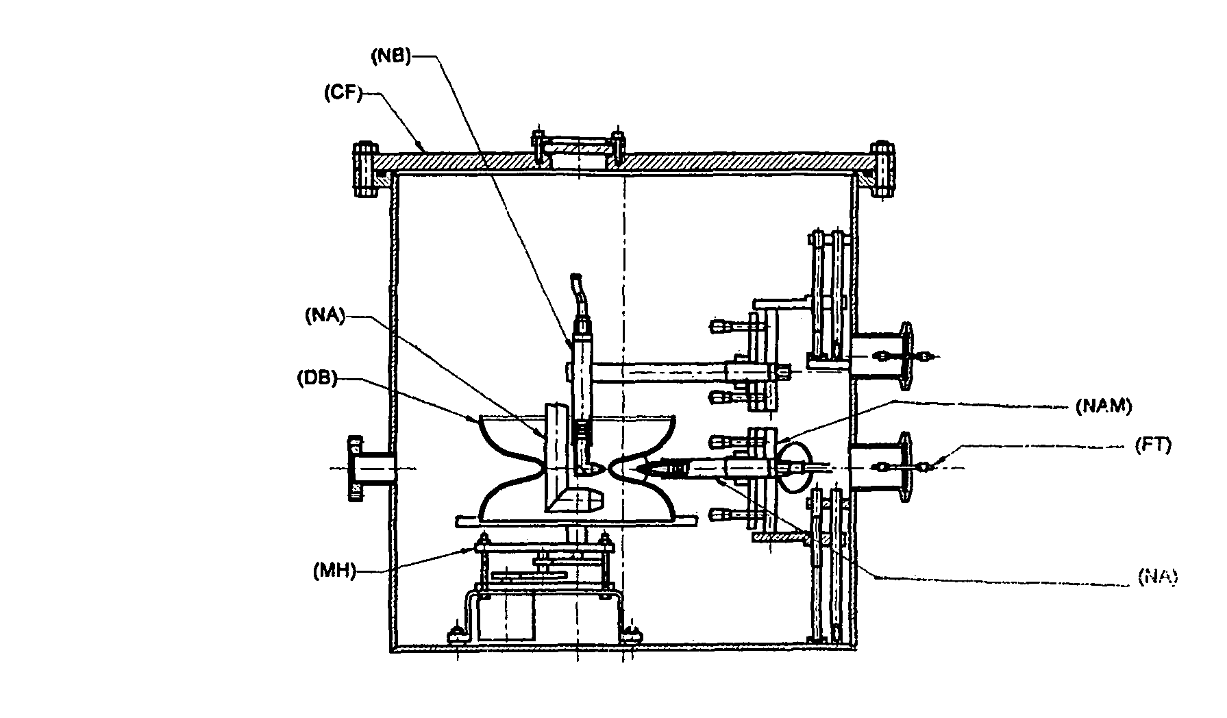
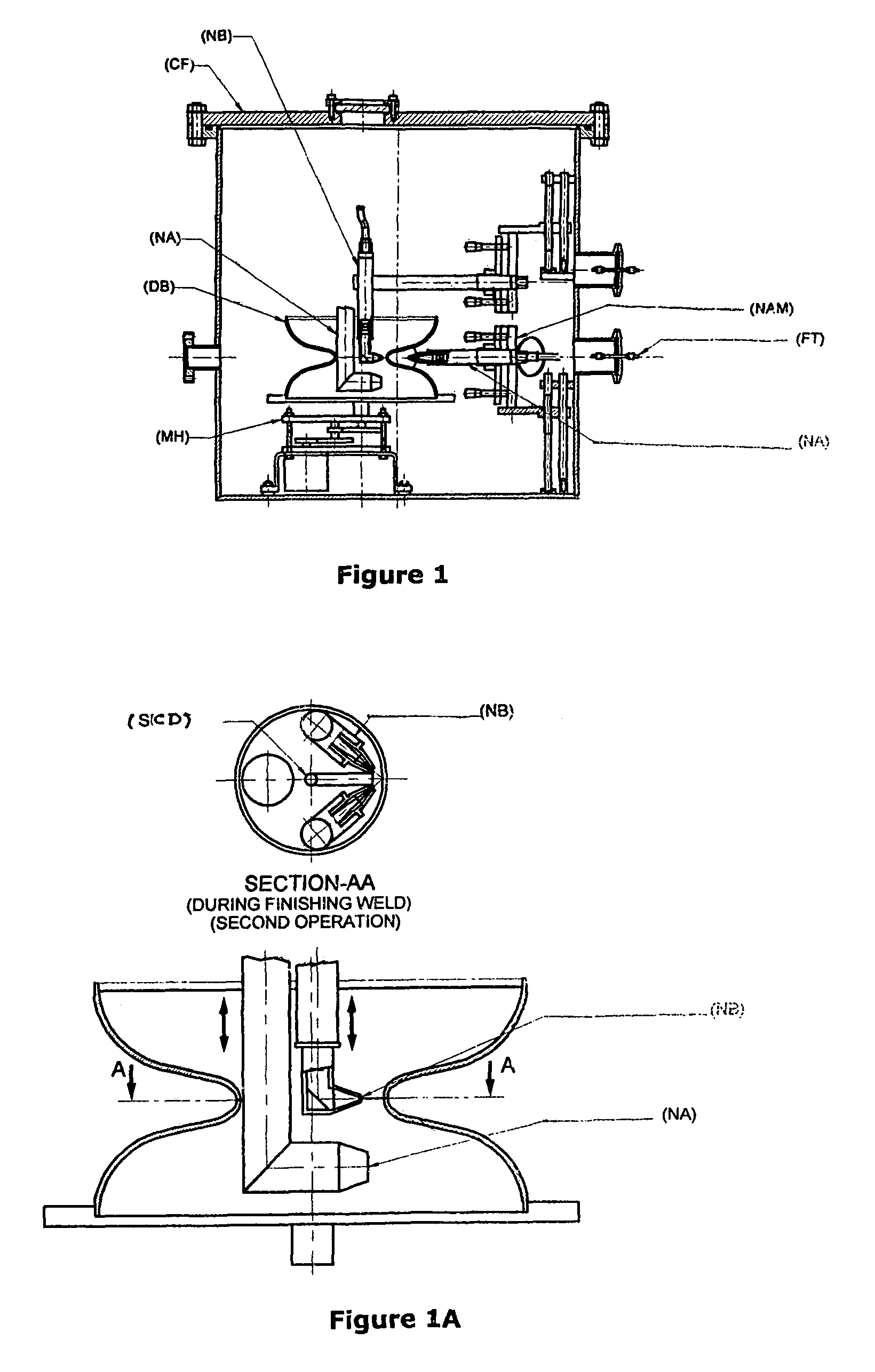
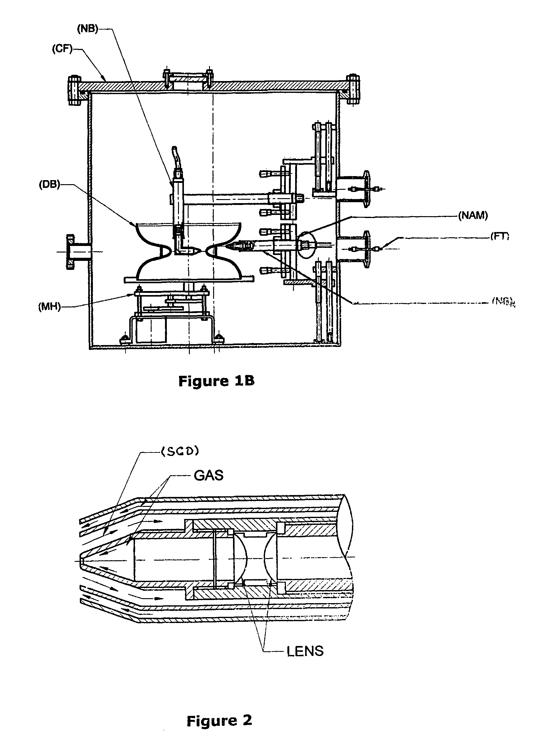
[0108]Reference is first invited to accompanying FIG. 1 which is a schematic illustration of the welding rig of Type 1 having a simple cylindrical vacuum chamber with motor driven attachments for holding the dumbbells to weld such as the iris joints to form dumbbells and stiffening rings on the dumbbells of SCRF cavity.

[0109]As clearly illustrated in said figure, the Type I rig basically involves the cylindrical vacuum chamber which accommodates a rotary mechanism for supporting a pair of half cells forming the dumbbell and adapted for rotary motion for facilitating the welding. For the purpose of effecting the welding from inside surface of the wall of the cavity in the RF field region, a nozzle is provided. Another set of welding nozzles is also provided for welding other parts of end group. All nozzles are provided with precise alignment mechanisms.

[0110]Importantly, the Type I rig is adapted to carry out the welding from inside surface of the wall of the half-cell within the RF ...


PUM

PropertyMeasurementUnit
thicknessaaaaaaaaaa
thicknessaaaaaaaaaa
angleaaaaaaaaaa

Abstract

Niobium or its alloy based Superconducting Radio Frequency (SCRF) Cavities involving atleast one laser beam welded components in the SCRF cavity welded from inside surface of the wall of cavity directed to achieving more than half the thickness to full depth penetration with minimum HAZ, minimizing distortion and shrinkage. The method ensures improved weld quality and surface finish substantially free of any weld defects. Also disclosed is the welding nozzle system and welding rigs adapted to facilitate such laser welding of the Niobium or its alloy based Superconducting Radio Frequency (SCRF) Cavities. The invention is thus directed to enhancing productivity, ensuring consistent quality and reliability, enhanced weld penetration with minimum HAZ, smooth finish of weld joints at possible reduced costs.

Description

CROSS REFERENCE TO RELATED APPLICATION[0001]The present application claims all benefits accruing under 35 U.S.C. §365(c) from the PCT International Application PCT / IN2009 / 000621, with an International Filing Date of Nov. 3, 2009, which claims the priority the entire contents of which are incorporated herein by reference.FIELD OF THE INVENTION[0002]The present invention relates to superconducting Radio Frequency (SCRF) Cavity and, in particular, to the fabrication of superconducting Radio Frequency (SCRF) Cavity involving laser welding with possible at least one welded joint welded from inside surface of the wall of the cavity to a depth of even more than half the thickness to full depth of the components welded with good strength and improved weld characteristics of the joints. More particularly, the invention is directed to Niobium and / or kits alloy based superconducting Radio Frequency (SCRF) Cavity fabrication involving possible laser weld from inside surface of the wall of cavit...

Claims


Application Information

Patent Timeline
Patent Type & Authority Patents(United States)
IPC IPC(8): H01L39/12H01L39/24B23K26/00B23K26/08B23K26/10B23K26/12B23K26/14B23K26/32B23K37/04B23K37/053H01L39/14H05H7/20H10N60/85H10N60/01H10N60/20
CPCB23K26/1224B23K26/0823B23K26/106B23K26/12B23K26/127B23K26/147B23K26/282B23K26/32B23K26/702B23K37/0435B23K37/0533H01L39/14H01L39/2406H05H7/20B23K2203/08B23K2103/08H10N60/0156H10N60/20
Inventor KHARE, PRASHANTUPADHYAY, BRAHMA NANDROY, SINDHUNIL BARMANPITHAWA, CHANDRAKANTSAHNI, VINOD CHANDRAGUPTA, PURUSHOTTAM DASKUSH, PRADEEP KUMAR
Owner SEC DEPT OF ATOMIC ENERGY
Learn More