
Source mask optimization to reduce stochastic effects

a source mask and stochastic effect technology, applied in the field of lithographic apparatuses and processes, can solve the problems of large cost of high-end patterning devices, application of opc is generally not possible,

Active Publication Date: 2015-12-15
ASML NETHERLANDS BV
View PDF29 Cites 23 Cited by
  • Summary
  • Abstract
  • Description
  • Claims
  • Application Information

AI Technical Summary

Benefits of technology

The patent text discusses the use of model-based optical proximity correction (OPC) in the design of semiconductor chips. The process involves creating a lithography recipe for a specific chip design using a single-beam machine and iterative iteration until the desired pattern is achieved. However, the application of OPC is not always perfect and there may be flaws in the pattern. To verify the quality of the design, a full-chip simulation using calibrated numerical process models is necessary. The text also mentions the use of off-axis illumination sources, which can improve patterning results. However, these sources provide less radiation intensity, so it is important to optimize the illumination source to achieve better results without compromising resolution. Finally, the text highlights the importance of source-patterning device optimization, which is becoming increasingly important for ensuring successful production of circuit designs on substrates.

Problems solved by technology

However, applying OPC is generally not an “exact science”, but an empirical, iterative process that does not always compensate for all possible proximity effect.
This is driven by the enormous cost of making high-end patterning devices, which run in the multi-million dollar range, as well as by the impact on turn-around time by reworking or repairing actual patterning devices once they have been manufactured.

Method used


Image

  • Source mask optimization to reduce stochastic effects
  • Source mask optimization to reduce stochastic effects
  • Source mask optimization to reduce stochastic effects

Examples


Embodiment Construction

[0033]Although specific reference may be made in this text to the manufacture of ICs, it should be explicitly understood that the description herein has many other possible applications. For example, it may be employed in the manufacture of integrated optical systems, guidance and detection patterns for magnetic domain memories, liquid-crystal display panels, thin-film magnetic heads, etc. The skilled artisan will appreciate that, in the context of such alternative applications, any use of the terms “reticle”, “wafer” or “die” in this text should be considered as interchangeable with the more general terms “mask”, “substrate” and “target portion”, respectively.

[0034]In the present document, the terms “radiation” and “beam” are used to encompass all types of electromagnetic radiation, including ultraviolet radiation (e.g. with a wavelength of 365, 248, 193, 157 or 126 nm) and EUV (extreme ultra-violet radiation, e.g. having a wavelength in the range 5-20 nm).

[0035]The term “optimizin...


PUM

PropertyMeasurementUnit
wavelengthaaaaaaaaaa
diameteraaaaaaaaaa

Abstract

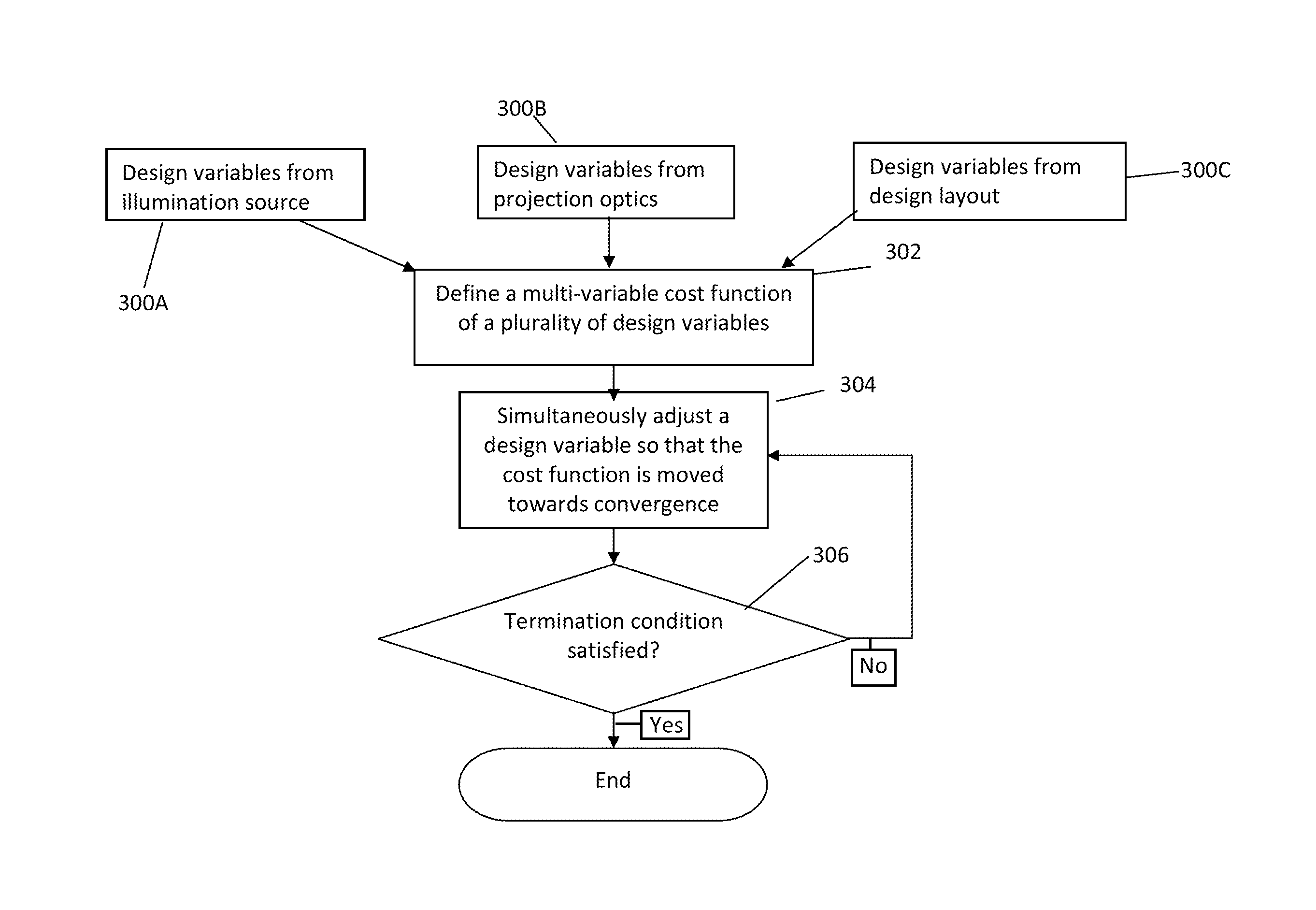
Disclosed herein is a computer-implemented method for improving a lithographic process for imaging a portion of a design layout onto a substrate using a lithographic projection apparatus, the method comprising defining a multi-variable cost function, the multi-variable cost function being a function of a stochastic effect of the lithographic process.

Description

CROSS-REFERENCE TO RELATED APPLICATIONS[0001]This application claims priority to U.S. Provisional Application No. 61 / 585,136 filed on Jan. 10, 2012, which is incorporated herein by reference in its entirety.TECHNICAL FIELD[0002]The description herein relates to lithographic apparatuses and processes, and more particularly to a tool to optimize an illumination source and / or patterning device / design layout for use in a lithographic apparatus or process.BACKGROUND[0003]A lithographic projection apparatus can be used, for example, in the manufacture of integrated circuits (ICs). In such a case, a patterning device (e.g., a mask) may contain or provide a circuit pattern corresponding to an individual layer of the IC (“design layout”), and this circuit pattern can be transferred onto a target portion (e.g. comprising one or more dies) on a substrate (e.g., silicon wafer) that has been coated with a layer of radiation-sensitive material (“resist”), by methods such as irradiating the target...

Claims


Application Information

Patent Timeline
Patent Type & Authority Patents(United States)
IPC IPC(8): G06F17/50G03F7/20G03F1/70
CPCG06F17/50G03F1/70G03F7/70125G03F7/70433G03F7/70441H01L21/0274G06F30/00G06F30/39
Inventor HANSEN, STEVEN GEORGE
Owner ASML NETHERLANDS BV
Learn More