
Escape routes

a technology of electromagnetic radiation and escape routes, applied in the field of electromagnetic radiation shielding, can solve the problems of void issues at the central ground pad, void problems, and excess flux applied, and achieve the effect of reducing/avoiding voids and reducing connection stresses

Active Publication Date: 2015-10-27
FLEXTRONICS AP LLC
View PDF52 Cites 3 Cited by
  • Summary
  • Abstract
  • Description
  • Claims
  • Application Information

AI Technical Summary

Benefits of technology

The patent text describes methods and devices to reduce voids between electronic components and PCB boards, as well as to lessen the connection stresses during solder joint formation. This is achieved by creating routes for the movement of flux and gases away from the solder joint during the process. The technical effects are improved performance and reliability of electronic assemblies.

Problems solved by technology

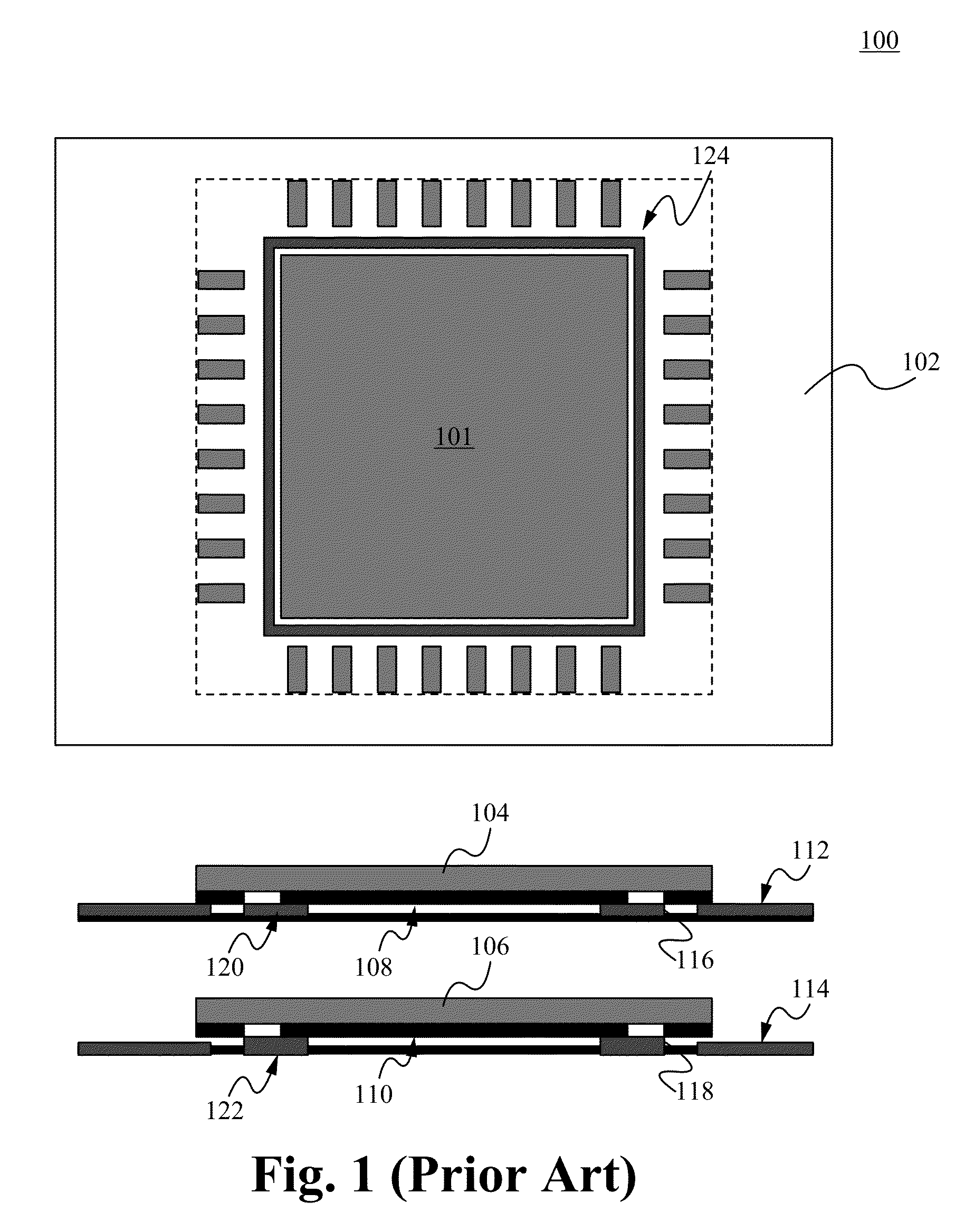
However, void issues at the central ground pads are problems for the BTC and other computer chips that are attached to printed circuit boards (PCB).
For example, a quad flat no-leads package (QFN) from automotive industry has a HiP (Head in Pillow) phenomenon with an occurrence of 90% of field failure in one pin connector, which generally result from the void issues.
Sometimes, the amount of flux applied is too much and the gases generated in the soldering process are often trapped underneath the components and pads affecting the reliability of the soldering joints.
Voids generated by the excess flux and the gases affect mechanical properties and reduce the integrity of the solder joint.

Method used


Image

  • Escape routes
  • Escape routes
  • Escape routes

Examples


Embodiment Construction

[0018]Reference is made in detail to the embodiments of the present invention, examples of which are illustrated in the accompanying drawings. While the invention is described in conjunction with the embodiments below, it is understood that they are not intended to limit the invention to these embodiments and examples. On the contrary, the invention is intended to cover alternatives, modifications and equivalents, which can be included within the spirit and scope of the invention as defined by the appended claims. Furthermore, in the following detailed description of the present invention, numerous specific details are set forth in order to more fully illustrate the present invention. However, it is apparent to one of ordinary skill in the prior art having the benefit of this disclosure that the present invention can be practiced without these specific details. In other instances, well-known methods and procedures, components and processes have not been described in detail so as not...


PUM

PropertyMeasurementUnit
diameteraaaaaaaaaa
heataaaaaaaaaa
pressureaaaaaaaaaa

Abstract

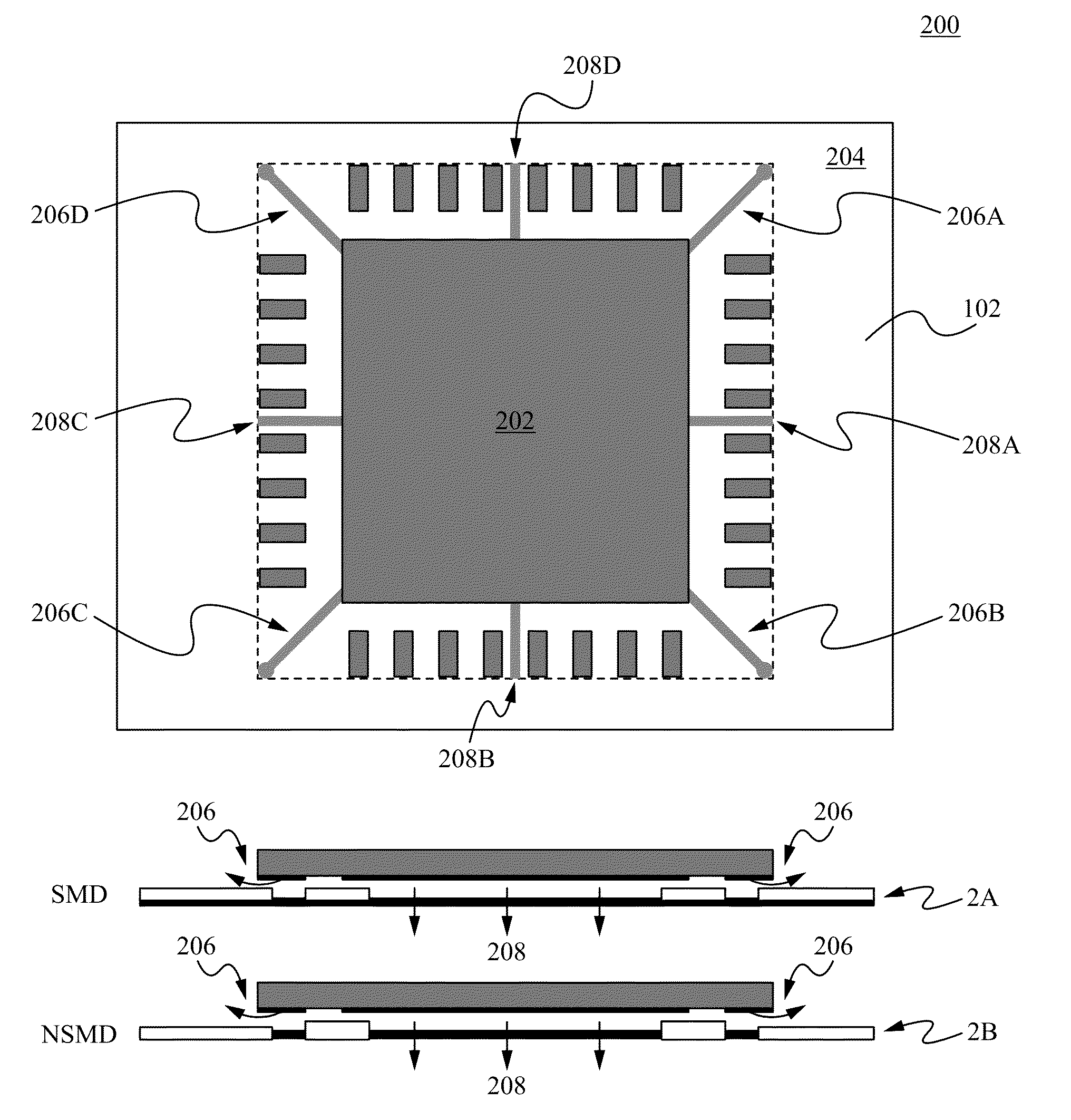
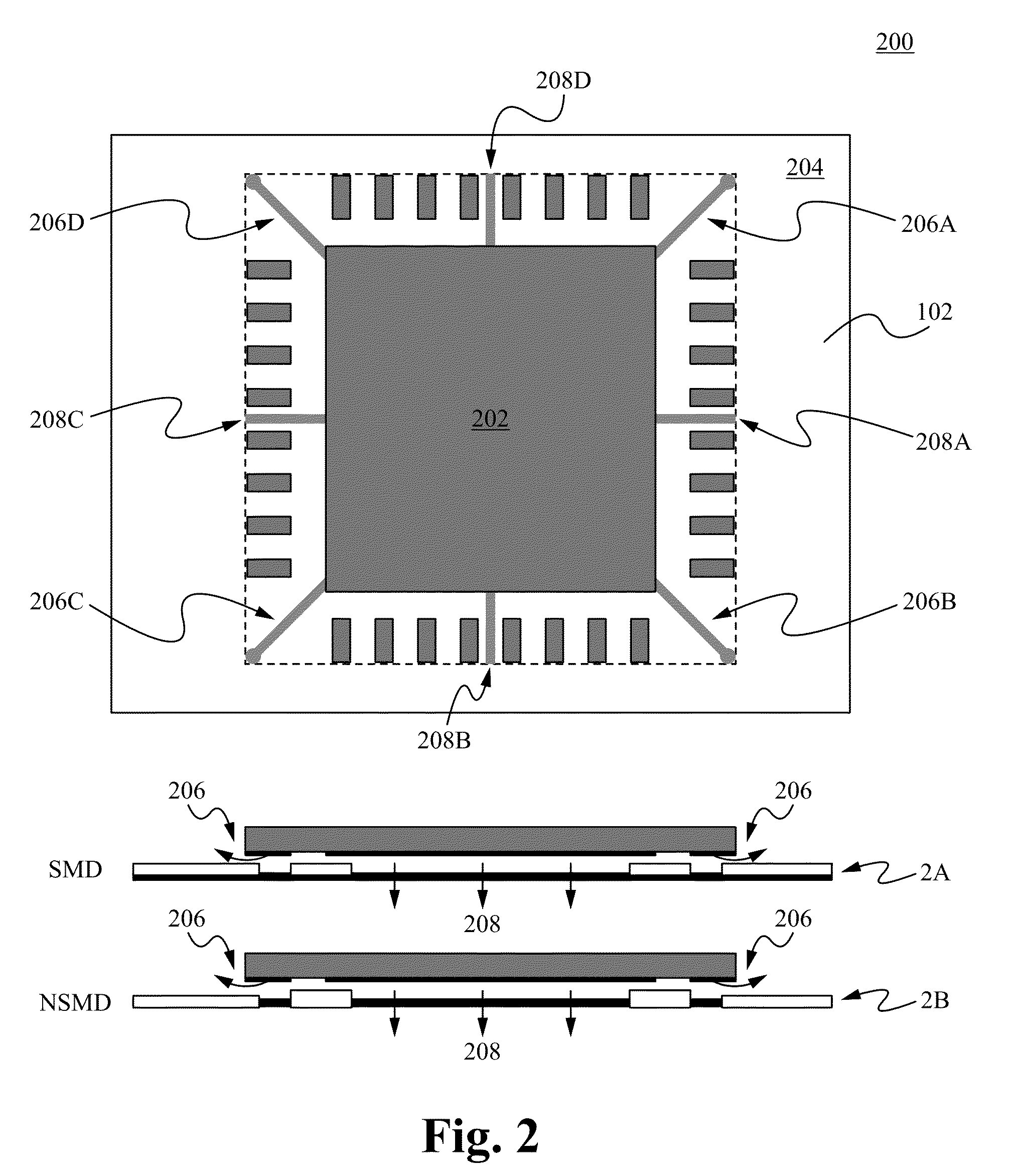
Methods of and devices for providing escaping routes for the flux and gases generated to move away from the solder joint in the process of solder joint formation.

Description

CROSS-REFERENCE TO RELATED APPLICATION(S)[0001]This application claims priority under 35 U.S.C. §119(e) of the U.S. Provisional Patent Application Ser. No. 61 / 772,978, filed Mar. 5, 2013 and titled, “ESCAPE ROUTES,” is hereby incorporated by reference in its entirety for all purposes.FIELD OF THE INVENTION[0002]The present invention relates to semiconductors. More specifically, the present invention relates to semiconductor assembly.BACKGROUND OF THE INVENTION[0003]With the popularity of the computers and the consumers' electronics, various electronic gadgets are becoming a necessity in our daily life. The electronic gadgets contain IC (integrated circuits) chips, such as bottom terminal components (BTC). BTC is getting more and more popular with its high connectivity speed. However, void issues at the central ground pads are problems for the BTC and other computer chips that are attached to printed circuit boards (PCB). For example, a quad flat no-leads package (QFN) from automotiv...

Claims


Application Information

Patent Timeline
Patent Type & Authority Patents(United States)
IPC IPC(8): H01L23/495H05K3/34H01L23/00H01L21/48H01L21/50H01L23/31
CPCH01L23/562H01L24/83H05K3/3436H05K3/3452H01L23/3107H01L2224/26122H01L2224/291H01L2224/83815H01L2924/1011H01L2924/15151H05K2201/09036H05K2201/10969H05K2203/1178H01L2924/00014H01L2924/014H01L2924/00012H01L2924/12042Y02P70/50H01L2924/00
Inventor LOPEZ, OMAR GARCIAAHUMADA QUINTERO, PEDRO ALEJANDROSECADA, ENRIQUE AVELARKURWA, MURADGONZALEZ, JUAN CARLOS
Owner FLEXTRONICS AP LLC
Learn More