GaN transistor with improved bonding pad structure and method of fabricating the same

a technology of gan transistors and bonding pads, which is applied in the field of gan transistors, can solve the problems of reduced chip life, increased production costs, and increased production costs, and achieves excellent reliability, high yield, and excellent reliability. the effect of a gan high-power transistor

Inactive Publication Date: 2015-10-20
ELECTRONICS & TELECOMM RES INST
View PDF6 Cites 0 Cited by
  • Summary
  • Abstract
  • Description
  • Claims
  • Application Information

AI Technical Summary

Benefits of technology

[0008]In this respect, the present inventors conducted research in order to solve the aforementioned problem, and found that when a structure and a process of a bonding pad is optimized in order to achieve excellent reliability of a GaN high-power transistor, adhesive force between a surface of GaN and the bonding pad is enhanced, so that it is possible to provide a GaN transistor with a high yield and excellent reliability, and completes the present invention.
[0009]The present invention has been made in an effort to provide a GaN transistor with an increased yield and excellent reliability by optimizing a structure of a bonding pad and enhancing adhesive force between a GaN surface and the bonding pad.
[0010]Further, the present invention has been made in an effort to provide a method of fabricating a GaN transistor with an increased yield and excellent reliability, which optimizes a structure and a process of a bonding pad during manufacturing of the GaN transistor to enhance adhesive force between a GaN surface and the bonding pad.
[0016]According to the embodiment of the present invention, adhesive force between a metal layer of the bonding pad and a GaN substrate is enhanced by forming the ohmic metal at the edges of the bonding pad during manufacturing of the GaN transistor, thereby minimizing a separation phenomenon of a pad layer during the wire-bonding or the back-side via-hole forming process, and improving reliability of a device.

Problems solved by technology

However, there is a case where adhesive force between the bonding pad and a wafer is poor according to a process condition, and during the wire bonding or the back-side via-hole forming process, the bonding pad is detached or the pad is separated during an operation, so that a life of a chip may be decreased.
Further, an original metal layer is formed at a center portion of the bonding pad, so that the wire-bonding or the back-side via-hole forming process is not influenced, and a separate mask is not used, so that an additional process cost is not generated.

Method used


Image

  • GaN transistor with improved bonding pad structure and method of fabricating the same
  • GaN transistor with improved bonding pad structure and method of fabricating the same
  • GaN transistor with improved bonding pad structure and method of fabricating the same

Examples


Embodiment Construction

[0024]Hereinafter, the present invention will be described in detail. The above objects, other objects, characteristics, and advantages of the present invention may be easily understood through the exemplary embodiment below related to the accompanying drawings. However, the present invention is not limited to the exemplary embodiments described herein, and may be implemented in various different forms. On the contrary, exemplary embodiments introduced herein are provided to make disclosed contents thorough and complete and sufficiently transfer the spirit of the present invention to those skilled in the art.

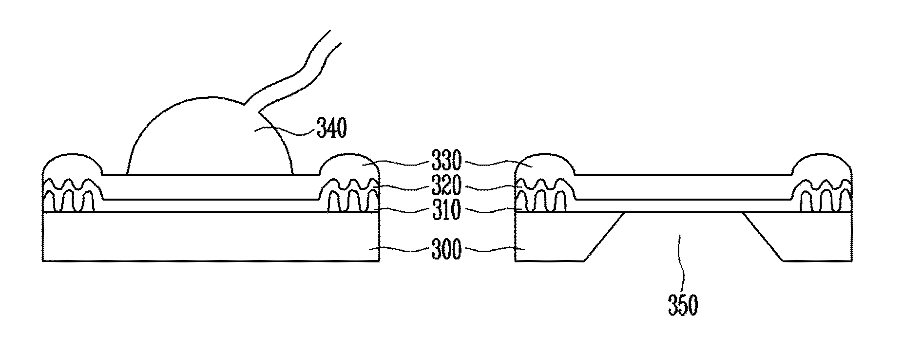
[0025]FIG. 1 is a cross-sectional view illustrating a structure of a GaN transistor.

[0026]Referring to FIG. 1, a GaN transistor includes an SiC substrate 10, a transition layer 20, a GaN buffer layer 30, an undoped GaN channel layer 40, an undoped AlGaN layer 50, an undoped GaN cap layer 60, a source electrode 70, a drain electrode 80, a silicon nitride layer 90, and a gate elec...


PUM


Abstract

The present invention relates to a GaN transistor, and a method of fabricating the same, in which a structure of a bonding pad is improved by forming an ohmic metal layer at edges of the bonding pad of a source, a drain, and a gate so as to be appropriate to wire-bonding or a back-side via-hole forming process. Accordingly, adhesive force between a metal layer of the bonding pad and a GaN substrate is enhanced by forming the ohmic metal at the edges of the bonding pad during manufacturing of the GaN transistor, thereby minimizing a separation phenomenon of a pad layer during the wire-bonding or back-side via-hole forming process, and improving reliability of a device.

Description

CROSS-REFERENCE TO RELATED APPLICATIONS[0001]This application is based on and claims priority from Korean Patent Application No. 10-2014-0006091, filed on Jan. 17, 2014, with the Korean Intellectual Property Office, the disclosure of which is incorporated herein in its entirety by reference.BACKGROUND[0002]1. Field[0003]The present invention relates to a GaN transistor and a method of fabricating the same. More particularly, the present invention relates to a GaN transistor, in which a bonding pad structure is improved to be appropriate to a wire bonding process or a back-side via-hole forming process to enhance adhesive force, thereby increasing a yield and improving reliability, and a method of fabricating the same.[0004]2. Discussion of Related Art[0005]Recently, a GaN transistor has been widely used as an ultrahigh frequency high-power device used in a radar for a war machine and a transceiver for a mobile communication base station. The high-power GaN transistor is generally mo...

Claims


Application Information

Patent Timeline
Patent Type & Authority Patents(United States)
IPC IPC(8): H01L33/00H01L23/00
CPCH01L24/05H01L24/03H01L2924/1033H01L2924/13091H01L2924/201H01L2224/03848H01L2224/0401H01L2224/05084H01L2224/05124H01L2224/05144H01L2224/05155H01L2224/05166H01L2924/37001H01L24/48H01L2224/03466H01L2224/04042H01L2224/05083H01L2224/05644H01L2224/48463H01L2924/00014H01L2924/10158H01L2924/1304H01L2924/1423H01L2224/0225H01L2224/45099A47J37/067A47J37/0786A47J36/022A47J36/04
Inventor KIM, HAE CHEONAHN, HO KYUNMIN, BYOUNG GUEYOON, HYUNG SUPLIM, JONG WON
Owner ELECTRONICS & TELECOMM RES INST
Why Eureka
Try Eureka