Electrostatic lens and charged particle beam apparatus using the same

a technology of electrostatic lenses and charged particle beams, applied in beam/ray focussing/reflecting arrangements, nanotechnology, electric discharge tubes, etc., can solve problems such as failure of wiring patterns, non-observation area to be generated, and difficulty in aligning electrostatic lenses. to achieve the effect of improving the irradiation accuracy of electron beams and improving throughpu

Inactive Publication Date: 2015-08-25
KYOCERA CORP
View PDF17 Cites 0 Cited by
  • Summary
  • Abstract
  • Description
  • Claims
  • Application Information

AI Technical Summary

Benefits of technology

This patent presents an electrostatic lens that improves the accuracy of electron beam irradiation while allowing for faster throughput. A charged particle beam apparatus that uses this electrostatic lens is also provided.

Problems solved by technology

When a plurality of electrostatic lenses are arranged, for example, in order to improve the throughput of the apparatus, it is difficult to align the plurality of electrostatic lenses since the electrostatic lenses are mechanically positioned.
Such a non-irradiation area often causes a non-observation area to be generated in the scanning electron microscope and a failure in wiring pattern to be occurred in the electron beam lithography apparatus.

Method used


Image

  • Electrostatic lens and charged particle beam apparatus using the same
  • Electrostatic lens and charged particle beam apparatus using the same
  • Electrostatic lens and charged particle beam apparatus using the same

Examples


Embodiment Construction

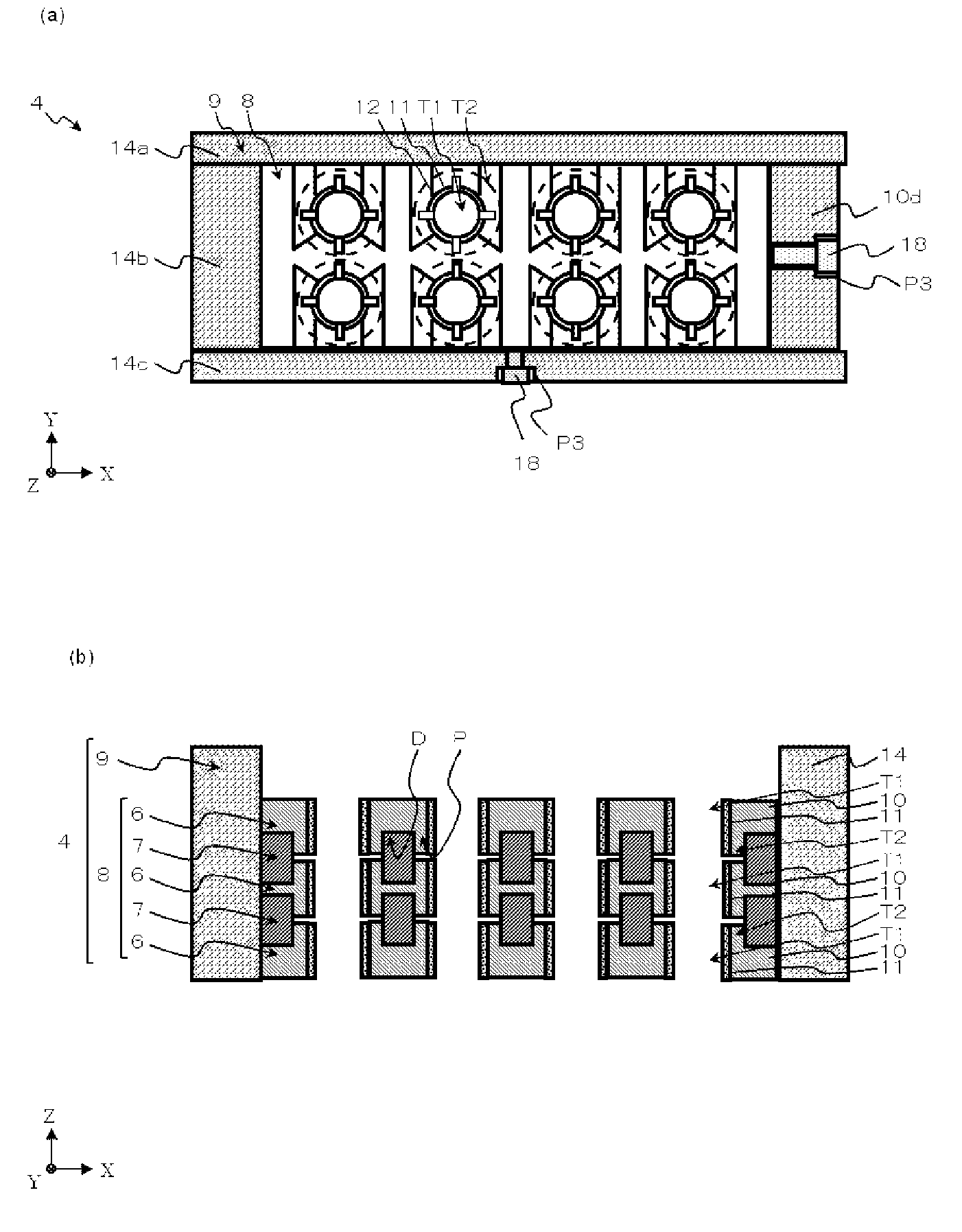
[0016]A charged particle beam apparatus which uses an electrostatic lens according to one embodiment of the present invention will be described in detail with reference to FIGS. 1 through 4.

[0017]A charged particle beam apparatus 1 shown in FIGS. 1(a) and 1(b) is, for example, used for a scanning electron microscope (SEM) that emits an electron beam E onto a surface of an object 2 such as a semiconductor wafer and a glass substrate and observes the object 2 using a generated secondary electron beam in a semiconductor manufacturing process or a flat panel display (FPD) manufacturing process, and an electron beam lithography apparatus for forming a fine wiring pattern on the object 2.

[0018]The charged particle beam apparatus 1 includes a plurality of electron guns 3 that emit a plurality of electron beams E, a plurality of electrostatic lenses 4 through which the plurality of electron beams E pass, and a stage 5 on which the object 2 is placed so that the plurality of electron beams E...


PUM


Abstract

To provide an electrostatic lens which improves an irradiation accuracy of an electron beam while satisfying the need for higher throughput. An electrostatic lens according to one embodiment of the present invention includes a substrate which includes an insulating plate in which a plurality of first through holes that allow an electron beam to pass through are formed, a plurality of electrodes that are formed on an inner wall of the plurality of first through holes, and a plurality of wirings that are formed on the insulating plate and are electrically connected to each of the electrodes, wherein the plurality of electrodes are electrically independent from each other.

Description

FIELD OF INVENTION[0001]The present invention relates to electrostatic lenses which are for example used for scanning electron microscopes in semiconductor manufacturing processes or flat panel display (FPD) manufacturing processes and charged particle beam apparatuses such as electron beam lithography apparatuses, and also relates to charged particle beam apparatuses using the electrostatic lenses.BACKGROUND[0002]Charged particle beam apparatuses are known to include, for example, scanning electron microscopes that emit an electron beam onto a surface of an object such as a semiconductor wafer and a glass substrate and use a generated secondary electron beam, and electron beam lithography apparatuses for forming a fine wiring pattern on an object.[0003]Japanese Unexamined Patent Application Publication No. 7-161329 discloses an electron beam apparatus which includes an electrostatic lens that allows a single axis electron beam to pass through.[0004]When a plurality of electrostatic...

Claims


Application Information

Patent Timeline
Patent Type & Authority Patents(United States)
IPC IPC(8): G21K5/04H01J37/30H01J3/18H01J37/28H01J37/12B82Y10/00B82Y40/00H01J37/317
CPCH01J37/12B82Y10/00B82Y40/00H01J3/18H01J37/28H01J37/3007H01J37/3177H01J2237/03H01J2237/1205
Inventor NOGUCHI, YUKIO
Owner KYOCERA CORP
Why Eureka
Try Eureka