
Stacked type semiconductor device and printed circuit board

a semiconductor device and printed circuit board technology, applied in printed circuit manufacturing, printed circuit stress/warp reduction, printed circuit aspects, etc., can solve the problem that the height of the bonding portion cannot be higher or equal to the height of the semiconductor element mounted, the strain value described above increases, and the interface between the solder ball and the metal post is easy to crack, so as to improve the reliability of bonding

Inactive Publication Date: 2015-08-18
CANON KK
View PDF15 Cites 0 Cited by
  • Summary
  • Abstract
  • Description
  • Claims
  • Application Information

AI Technical Summary

Benefits of technology

The solution effectively reduces strain on the solder material by distributing the shear load through the voids in the metal particle aggregate, ensuring the height of the joint material and enhancing the reliability of the bonding, allowing for a smaller semiconductor device area while maintaining reliability.

Problems solved by technology

Therefore, when the diameter of the solder ball, which is the bonding portion, is simply reduced in order to downsize the semiconductor device, the height of the bonding portion cannot be higher than or equal to the height of the semiconductor element mounted on the lower interposer.
However, in the case of the configuration described in PTL 1, when the diameter of the solder ball is decreased, the strain value described above increases and cracks tend to occur in the interface between the solder ball and the metal post.
In particular, a shear stress is concentrated on the interface between the solder ball and the metal post where the physical property of materials drastically changes, so that there is a problem that long term reliability cannot be ensured.

Method used


Image

  • Stacked type semiconductor device and printed circuit board
  • Stacked type semiconductor device and printed circuit board
  • Stacked type semiconductor device and printed circuit board

Examples


first embodiment

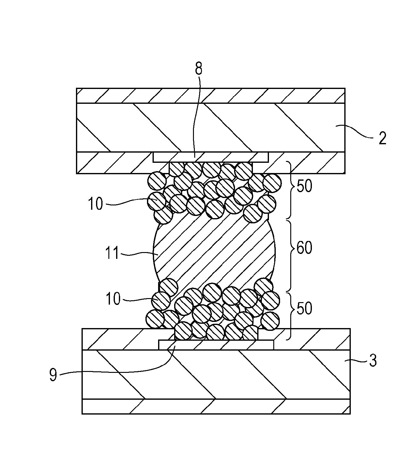
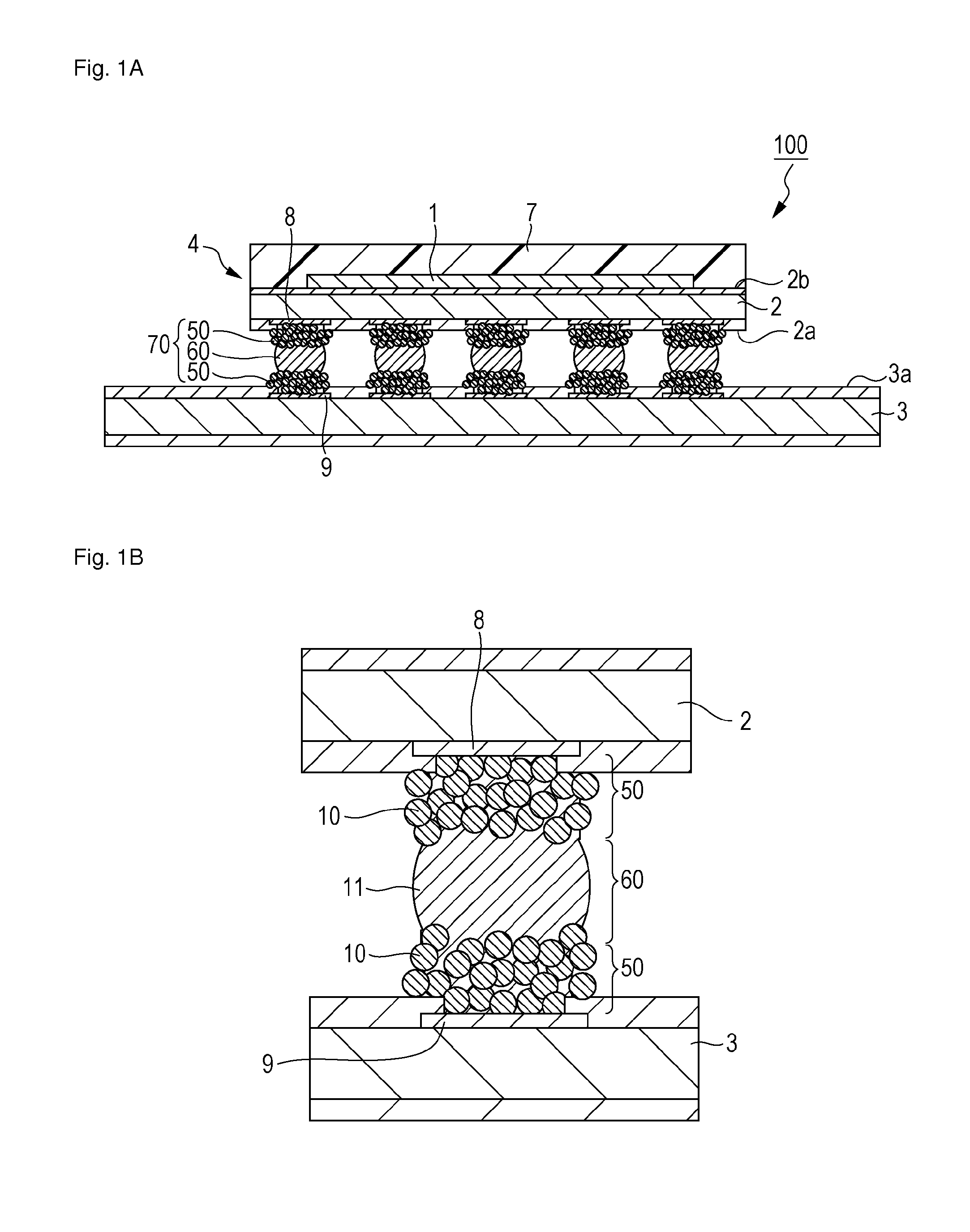
[0039]FIGS. 1A and 1B are illustrations showing a schematic configuration of a printed circuit board according to a first embodiment of the present invention. FIG. 1A is a schematic cross-sectional view of the entire printed circuit board. FIG. 1B is a partial enlarged view of a bonding portion.

[0040]As shown in FIG. 1A, a printed circuit board 100 includes a printed wiring board (mother board) 3 as a wiring substrate and a semiconductor device 4 mounted on the printed wiring board 3.

[0041]The semiconductor device 4 is a semiconductor package having a semiconductor element 1 including a semiconductor chip such as a CPU and an interposer 2 as a wiring substrate on which the semiconductor element 1 is mounted. One surface (one side) 2a of the interposer 2 and one surface (one side) 3a of the printed wiring board 3 face each other. The semiconductor element 1 is mounted on the other surface 2b of the interposer 2 and sealed along with the surface 2b by a sealing resin 7.

[0042]A plurali...

second embodiment

[0062]Next, a printed circuit board to which a joint material according to a second embodiment of the present invention is applied will be described. FIGS. 3A and 3B are illustrations showing a schematic configuration of the printed circuit board according to the second embodiment of the present invention. FIG. 3A is a schematic cross-sectional view of the entire printed circuit board. FIG. 3B is a partial enlarged view of a bonding portion. The same components as those in the embodiment described above are given the same reference numerals and the descriptions thereof will be omitted.

[0063]In the first embodiment, a case is described in which the metal particle aggregate 10 is provided to the electrode pad 8 of the interposer 2 and the electrode pad 9 of the printed wiring board (mother board) 3 to form the metal layers 50. The metal layer 50 may be formed on at least one of the electrode pad 8 of the interposer 2 and the electrode pad 9 of the printed wiring board (mother board) 3...

third embodiment

[0073]Next, a printed circuit board to which a joint material according to a third embodiment of the present invention is applied will be described. FIGS. 5A and 5B are illustrations showing a schematic configuration of the printed circuit board according to the third embodiment of the present invention. FIG. 5A is a schematic cross-sectional view showing the entire printed circuit board. FIG. 5B is a partial enlarged view of a bonding portion. The same components as those in the embodiments described above are given the same reference numerals and the descriptions thereof will be omitted.

[0074]As shown in FIG. 5A, a printed circuit board 100B includes the interposer 2 of the semiconductor device 4B and the printed wiring board 3, which are bonded together by a joint material 70B. As shown in FIG. 5B, the joint material 70B includes a metal layer 50B having a porous metal particle aggregate 10B formed on the electrode pads 9 of the printed wiring board 3 and a solder layer 60B forme...


PUM


Abstract

The printed circuit board (100) includes the interposer (2) where the semiconductor element (1) is mounted and the electrode pad (8) is formed on one surface, the printed wiring board (3) where the electrode pad (9) is formed on one surface facing the interposer (2), and the joint material (70) for bonding the electrode pads (8) and (9). The joint material (70) includes the solder layer (60) formed by the solder material (11) and the metal layers (50), (50) provided to the electrode pads (8) and (9). Each metal layer (50) includes the metal particle aggregate (10) in which metal particles are integrated with voids and is formed by filling the voids in the metal particle aggregate (10) with melted solder material (11). It is possible to ensure the height of the solder, improve reliability of the bonding, and downsize the semiconductor device by using such joint material.

Description

TECHNICAL FIELD[0001]The present invention relates to a stacked type semiconductor device and a printed circuit board which include a joint material that bonds electrode pads together.BACKGROUND ART[0002]In recent years, digital devices such as a digital camera and a digital video camera are becoming lighter, thinner, shorter, and smaller and semiconductor devices in which many electronic components are mounted in a smaller space are used. A stacked type semiconductor device in which a plurality of semiconductor devices are stacked attracts attention. The stacked type semiconductor device is formed by bonding a semiconductor package by a joint material such as solder onto another semiconductor package in which a semiconductor element is mounted on an interposer.[0003]The mainstream of semiconductor devices is a semiconductor package of BGA (Ball Grid Array) in which solder balls are used as joint materials which are external connection electrode. Among the BGAs, a semiconductor pack...

Claims


Application Information

Patent Timeline
Patent Type & Authority Patents(United States)
IPC IPC(8): H01L23/48H01L25/10H01L23/488H01L23/498H05K3/34H05K1/09H01L23/485H05K1/02
CPCH01L25/105H01L23/488H01L23/49816H05K3/3484H01L23/485H01L2225/1023H01L2225/1058H01L2924/014H01L2924/01029H01L2924/15311H01L2924/15331H05K1/0271H05K1/09H05K2201/10378H05K2201/10734H05K2203/0425H01L23/49811H01L23/49883H01L21/4867H01L2924/3511H01L2224/32225H01L2924/19101H01L2924/37001H01L2924/0002H05K3/3485H01L2924/0001
Inventor FUJISAWA, YOSHITOMO
Owner CANON KK
Learn More