Gate structure including a metal silicide pattern in which an upper surface portion of the metal silicide pattern includes concavo-convex portions and semiconductor devices including the same

a metal silicide pattern and gate structure technology, applied in the field of semiconductor devices, can solve the problems of metal silicide pattern formation that is difficult to achieve, the resistance of the gate electrode may be locally increased, and the semiconductor device having the metal silicide pattern as a part of the gate electrode may malfunction, etc., to achieve good electrical properties of semiconductor devices, the resistance difference between the gate structure may be very small, and the resistance may be good

Active Publication Date: 2015-07-07
SAMSUNG ELECTRONICS CO LTD
View PDF10 Cites 0 Cited by
  • Summary
  • Abstract
  • Description
  • Claims
  • Application Information

AI Technical Summary

Benefits of technology

[0026]As described above, the gate structure included in the semiconductor device in accordance with the present inventive concept may include a metal silicide pattern having a uniform thickness. Accordingly, the gate structure may have a low resistance. In addition, a resistance difference between the gate structures may be very small. The electrical property of the semiconductor device may be good and an operation defect may be decreased.

Problems solved by technology

A semiconductor device may include gate electrodes having various line widths, and forming metal silicide patterns having a uniform thickness may be difficult.
When the metal silicide patterns having non-uniform thicknesses are formed, resistances of the gate electrodes may be locally increased and a semiconductor device having the metal silicide patterns as part of the gate electrodes may malfunction.

Method used


Image

  • Gate structure including a metal silicide pattern in which an upper surface portion of the metal silicide pattern includes concavo-convex portions and semiconductor devices including the same
  • Gate structure including a metal silicide pattern in which an upper surface portion of the metal silicide pattern includes concavo-convex portions and semiconductor devices including the same
  • Gate structure including a metal silicide pattern in which an upper surface portion of the metal silicide pattern includes concavo-convex portions and semiconductor devices including the same

Examples


Embodiment Construction

[0035]Various example embodiments will be described more fully hereinafter with reference to the accompanying drawings, in which some example embodiments are shown. The present inventive concept may, however, be embodied in many different forms and should not be construed as limited to the example embodiments set forth herein. In the drawings, the sizes and relative sizes of layers and regions may be exaggerated for clarity.

[0036]Hereinafter, example embodiments on semiconductor devices and methods of manufacturing the semiconductor devices will be explained in further detail.

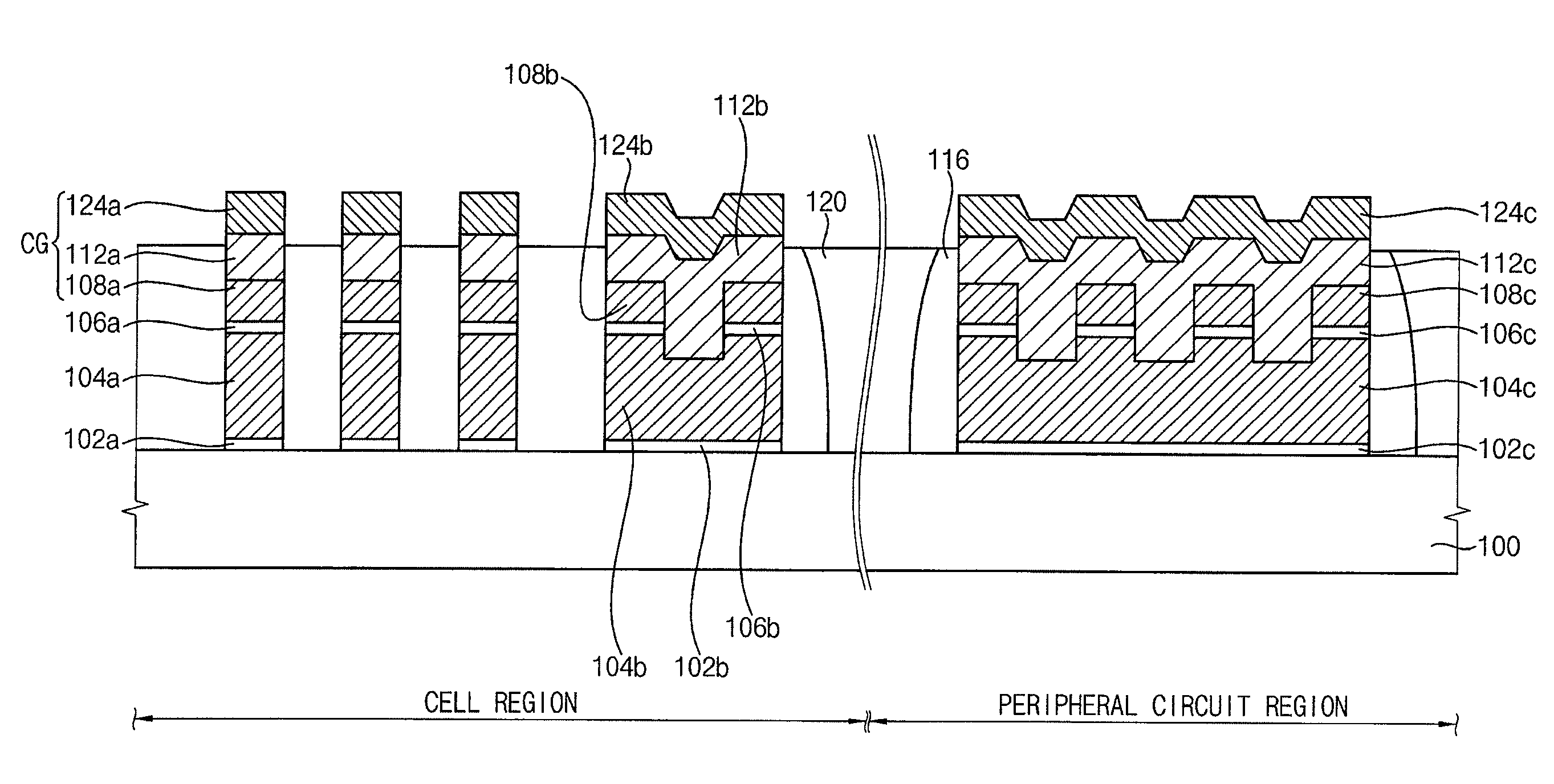
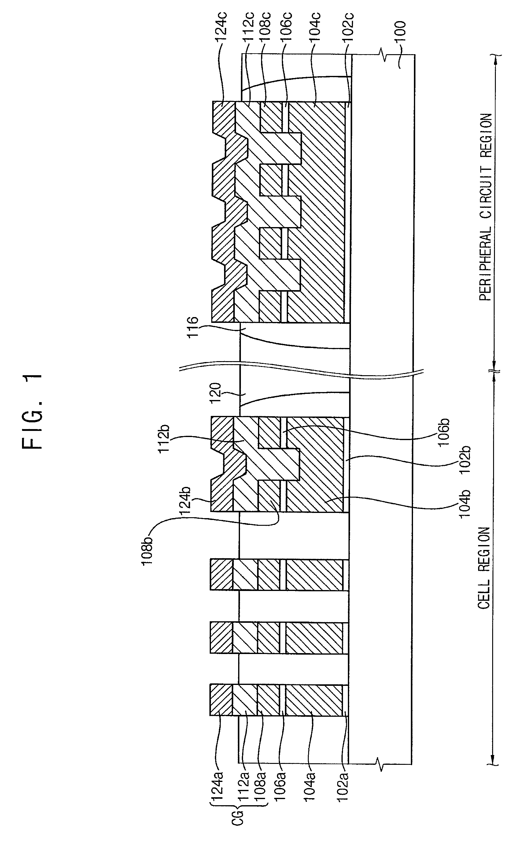
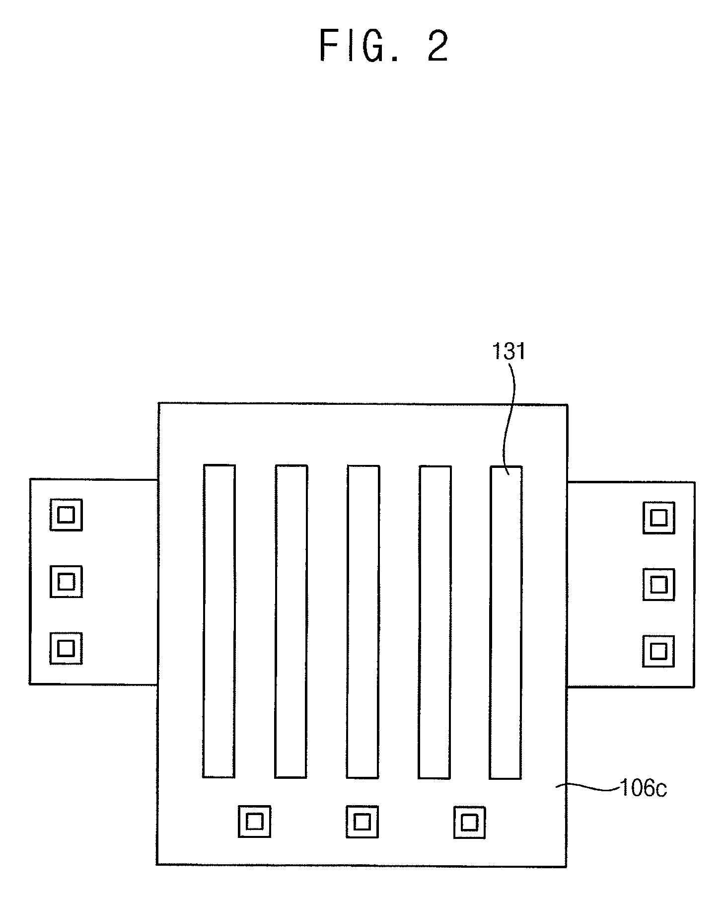
[0037]FIG. 1 is a cross-sectional view illustrating a semiconductor device in accordance with example embodiments. FIG. 2 is a plan view illustrating a dielectric layer portion in a gate electrode of a transistor in a peripheral circuit region included in the semiconductor device illustrated in FIG. 1.

[0038]In accordance with an embodiment of the inventive concept, the semiconductor device illustrated in FIG. 1...


PUM


Abstract

In a semiconductor device, a first gate structure is provided in a cell transistor region and includes a floating gate electrode, a first dielectric layer pattern, and a control gate electrode including a first metal silicide pattern. A second gate structure is provided in a selecting transistor region and includes a first conductive layer pattern, a second dielectric layer pattern, and a first gate electrode including a second metal silicide pattern. A third gate structure is provided in a peripheral circuit region and includes a second conductive layer pattern, a third dielectric layer pattern including opening portions on the second conductive layer pattern, and a second gate electrode including a concavo-convex portion at an upper surface portion thereof and a third metal silicide pattern. The third metal silicide pattern has a uniform thickness.

Description

CROSS-REFERENCE TO RELATED APPLICATIONS[0001]This application claims priority under 35 USC §119 to Korean Patent Application No. 10-2011-0015472, filed on Feb. 22, 2011 in the Korean Intellectual Property Office (KIPO), the contents of which are herein incorporated by reference in their entirety.BACKGROUND[0002]1. Field[0003]Example embodiments relate to semiconductor devices and methods of manufacturing the same. More particularly, example embodiments relate to semiconductor devices including a gate electrode and methods of manufacturing the same.[0004]2. Discussion of the Related Art[0005]To manufacture a highly integrated semiconductor device, a gate electrode having a low resistance may be required. A portion of the gate electrode may be formed as a metal silicide pattern. A semiconductor device may include gate electrodes having various line widths, and forming metal silicide patterns having a uniform thickness may be difficult. When the metal silicide patterns having non-unifo...

Claims


Application Information

Patent Timeline
Patent Type & Authority Patents(United States)
IPC IPC(8): H01L27/115H01L21/28H01L21/8234
CPCH01L27/11529H01L21/28273H01L21/823437H01L21/823443H01L21/823456H01L29/40114H10B41/41H01L21/28052H01L29/4975H01L29/495H01L29/788H01L29/42328H10B41/35
Inventor LEE, SUNG-HUNKIM, KI-YONGPARK, SUNG-WOOKLEE, GYU-YEOL
Owner SAMSUNG ELECTRONICS CO LTD
Why Eureka
Try Eureka