Silicon carbide epitaxial substrate and method of manufacturing silicon carbide epitaxial substrate

a technology of which is applied in the direction of crystal growth process, polycrystalline material growth, transportation and packaging, etc., can solve the problems of difficult to sufficiently reduce the background concentration of nitrogen in the silicon carbide epitaxial layer obtained, and difficult to achieve good surface quality. , the effect of reducing the background concentration and uniform nitrogen concentration distribution in the plan

Active Publication Date: 2015-06-16
SUMITOMO ELECTRIC IND LTD
View PDF7 Cites 1 Cited by
  • Summary
  • Abstract
  • Description
  • Claims
  • Application Information

AI Technical Summary

Benefits of technology

[0011]According to the present invention, there can be provided a silicon carbide epitaxial substrate that has good surface quality, that has a sufficiently reduced background concentration, and that has a uniform in-plane distribution of nitrogen concentration.

Problems solved by technology

However, the inventors of the present application have found that even though the nitrogen concentration in the film member covering the susceptor is made low as described in Japanese Patent Laying-Open No. 2006-028625, it may be difficult to sufficiently reduce the background concentration of nitrogen in a silicon carbide epitaxial layer obtained through epitaxial growth and having good surface quality.
Also, the inventors of the present application have found that under the above-described growth condition, nitrogen is likely to be captured in the silicon carbide epitaxial substrate and it is difficult to sufficiently reduce the background concentration of nitrogen in the obtained silicon carbide epitaxial layer using the technique of Japanese Patent Laying-Open No. 2006-028625.

Method used


Image

  • Silicon carbide epitaxial substrate and method of manufacturing silicon carbide epitaxial substrate
  • Silicon carbide epitaxial substrate and method of manufacturing silicon carbide epitaxial substrate
  • Silicon carbide epitaxial substrate and method of manufacturing silicon carbide epitaxial substrate

Examples


example 1

[0103]The following describes an example of the present invention.

[0104]1. Evaluation Samples

[0105](i) Example Sample 1

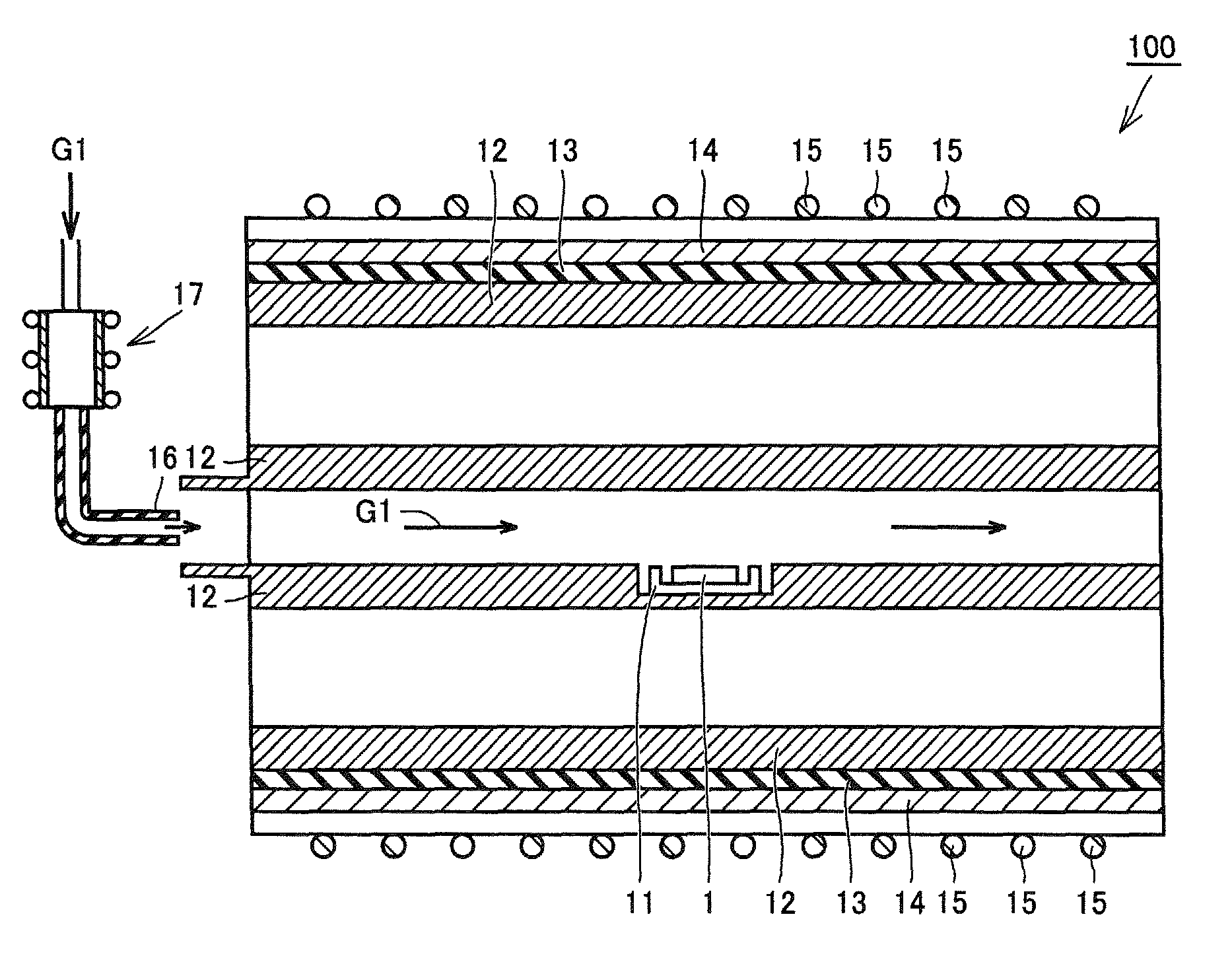
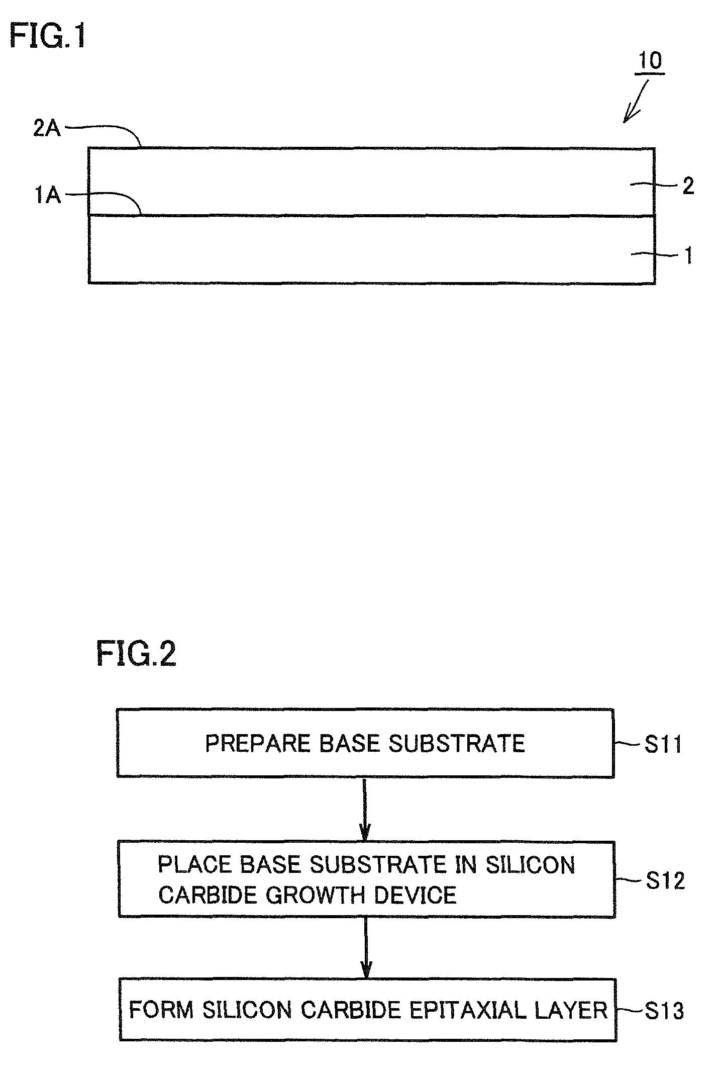
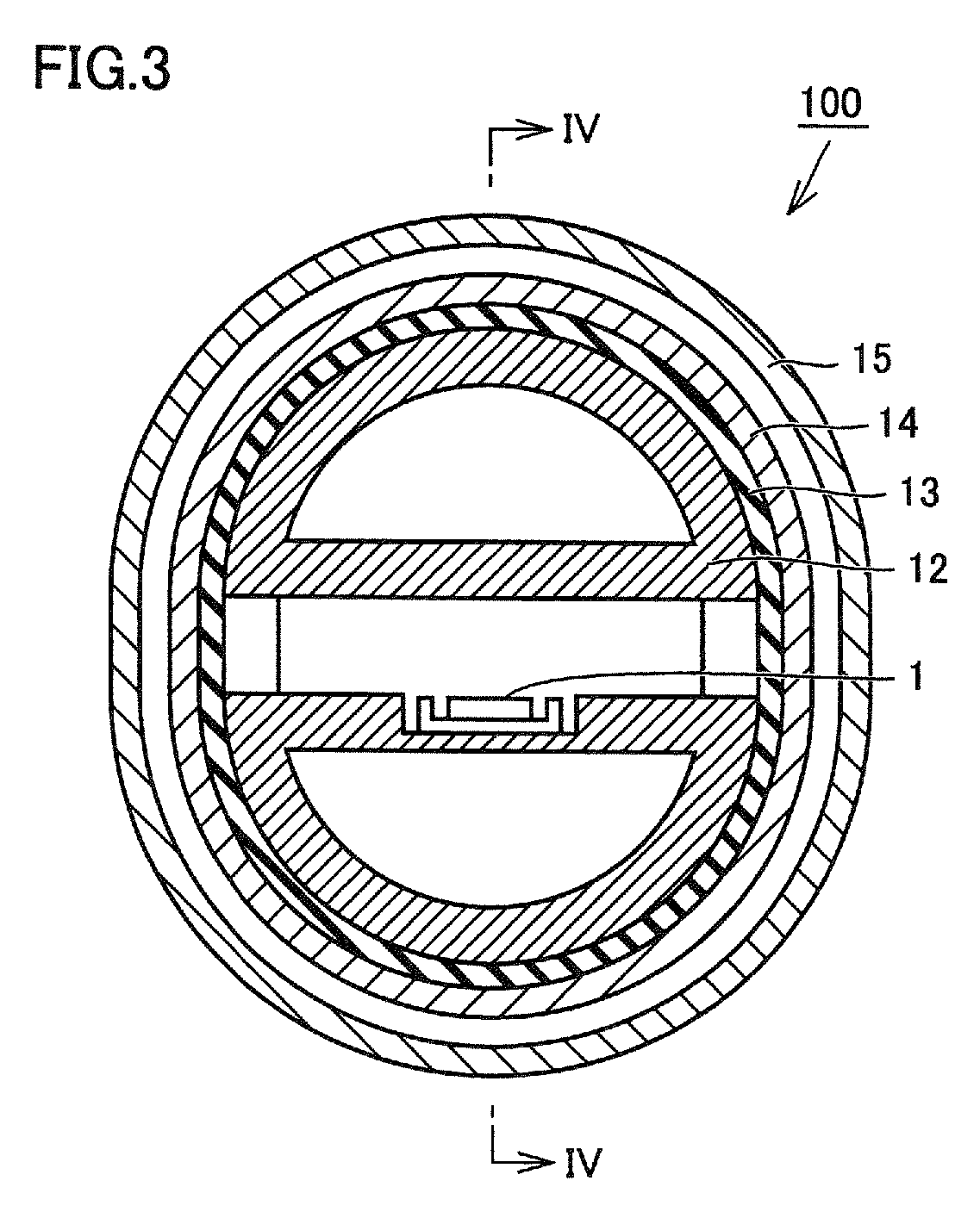
[0106]First, a base substrate made of silicon carbide and having an outer diameter of 150 mm and a thickness of 350 μm was prepared.

[0107]Next, the silicon carbide growth device according to the present embodiment was used to form, on the first main surface of the base substrate, a silicon carbide epitaxial layer having an impurity concentration of 1.0×1015 cm−3 and a thickness of 15 μm. For the substrate holder of the silicon carbide growth device, there was employed a substrate holder including: a substrate holder body having a nitrogen concentration of 2 ppm; and a holder coating portion having a nitrogen concentration of 0.4 ppm. For the heat generator, there was employed a heat generator including: a heat generator body having a nitrogen concentration of 2 ppm; and a heat generator coating portion having a nitrogen concentration of 0.4 ppm. Introduced into the ...


PUM

PropertyMeasurementUnit
outer diameteraaaaaaaaaa
surface roughnessaaaaaaaaaa
temperatureaaaaaaaaaa

Abstract

A silicon carbide epitaxial substrate having a main surface (second main surface) includes: a base substrate; and a silicon carbide epitaxial layer formed on the base substrate and including the main surface (second main surface), the second main surface having a surface roughness of 0.6 nm or less, a ratio of standard deviation of a nitrogen concentration in the silicon carbide epitaxial layer at a surface layer including the main surface (second main surface) within a plane of the silicon carbide epitaxial substrate to an average value of the nitrogen concentration in the silicon carbide epitaxial layer at the surface layer within the plane of the silicon carbide epitaxial substrate being 15% or less.

Description

BACKGROUND OF THE INVENTION[0001]1. Field of the Invention[0002]The present invention relates to a silicon carbide epitaxial substrate, a method of manufacturing the silicon carbide epitaxial substrate, a method of manufacturing a silicon carbide semiconductor device, a silicon carbide growth device, and a silicon carbide growth device member. In particular, the present invention relates to a silicon carbide epitaxial substrate for a silicon carbide semiconductor device required to have a high breakdown voltage, a method of manufacturing the silicon carbide epitaxial substrate, a method of manufacturing the silicon carbide semiconductor device, a silicon carbide growth device, and a silicon carbide growth device member.[0003]2. Description of the Background Art[0004]Epitaxial growth of a compound semiconductor such as silicon carbide on a substrate needs to be performed by reacting a treatment gas (source material gas or the like) under a high temperature.[0005]Conventionally, in an...

Claims


Application Information

Patent Timeline
Patent Type & Authority Patents(United States)
IPC IPC(8): C23C16/00C30B25/12C30B29/36
CPCC30B25/12C30B29/36C30B25/08C30B25/20Y10T428/21Y10T428/24355C30B29/64
Inventor GENBA, JUNNISHIGUCHI, TARODOI, HIDEYUKIMATSUSHIMA, AKIRA
Owner SUMITOMO ELECTRIC IND LTD
Why Eureka
Try Eureka