Control device and method for actuating a semiconductor switch

a control device and switch technology, applied in the direction of power conversion systems, electrical devices, pulse generators, etc., can solve the problems of self-excited interference transmitters, unavoidable input capacitances, and inability to control the output voltage of the control device,

Active Publication Date: 2015-05-26
MARKS WALTER
View PDF1 Cites 0 Cited by
  • Summary
  • Abstract
  • Description
  • Claims
  • Application Information

AI Technical Summary

Benefits of technology

This patent is about a new way to control the switching of a semiconductor switch, which prevents interference and ring gain. The control connection of the switch is provided with a high current intensity that changes quickly with the rate of voltage change. This means that the time it takes for the current to increase or decrease is always faster than the time it takes for the voltage to change. This also prevents the voltage from causing interference or ring gain in the semiconductor switch. Additionally, the voltage-current converter is designed with ohmic resistances to minimize inductive effects and reduce interference. Overall, this patent provides a faster and more efficient way to control semiconductor switches while minimizing interference and ring gain.

Problems solved by technology

This is due to the fact that, in the case of current sources controllable by voltage, there are always unavoidable input capacitances, for example due to the high input resistance and the necessary electrical connections of the components of the current sources.
Here it may occur that the shift of the phasing between voltage and current of the voltage-controlled current source reaches a value of 1 or more than 1 for fractions of the changing freewheeling voltage after conversion into a control current for the gate electrode and from this a fraction of the control voltage occurring between gate and source together with the voltage gain in the semiconductor switch, so that there is an unacceptable ring gain resulting in a self-excited interference transmitter which emits incompatible interference power into the environment.

Method used


Image

  • Control device and method for actuating a semiconductor switch
  • Control device and method for actuating a semiconductor switch
  • Control device and method for actuating a semiconductor switch

Examples


second embodiment

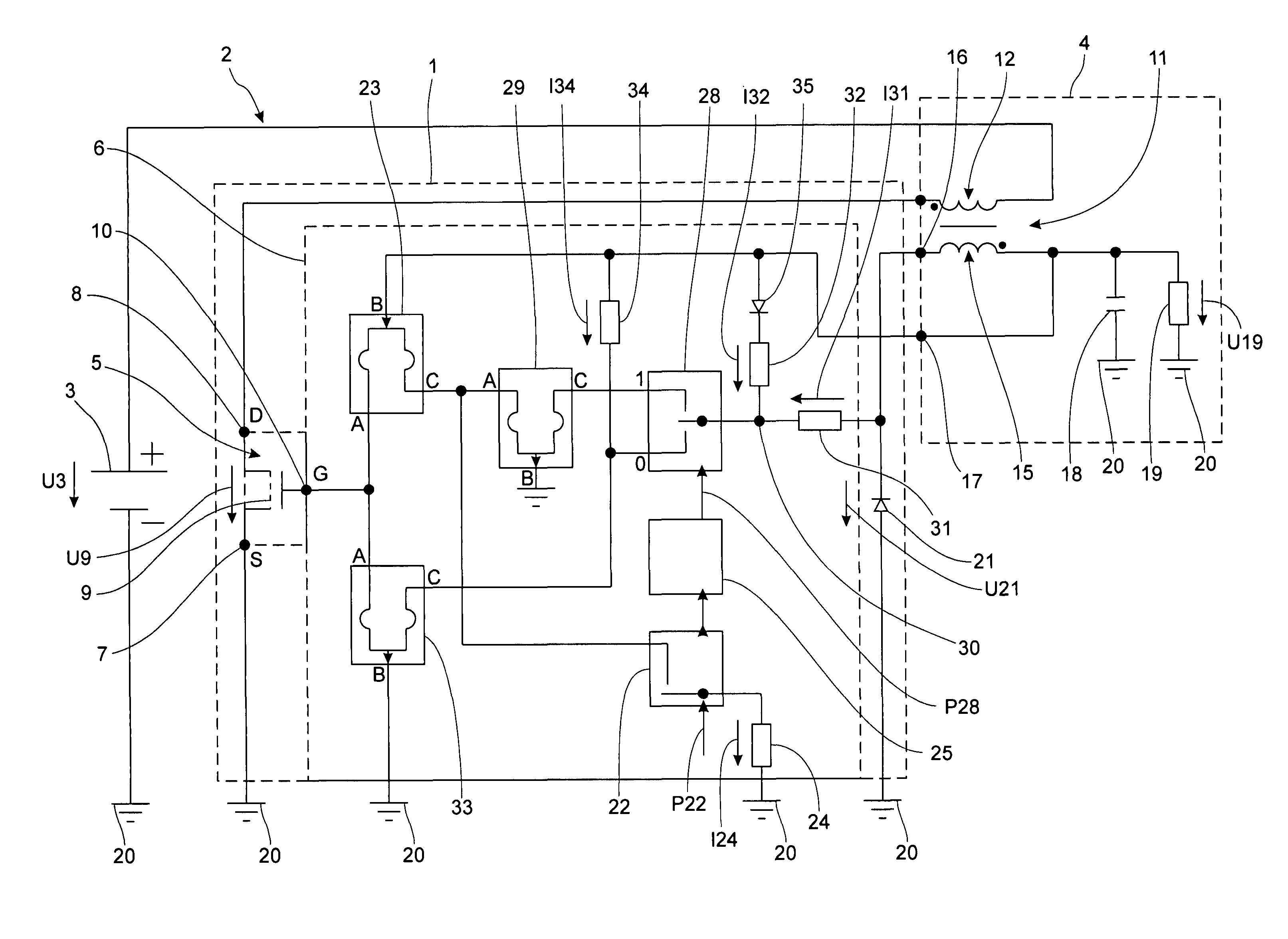
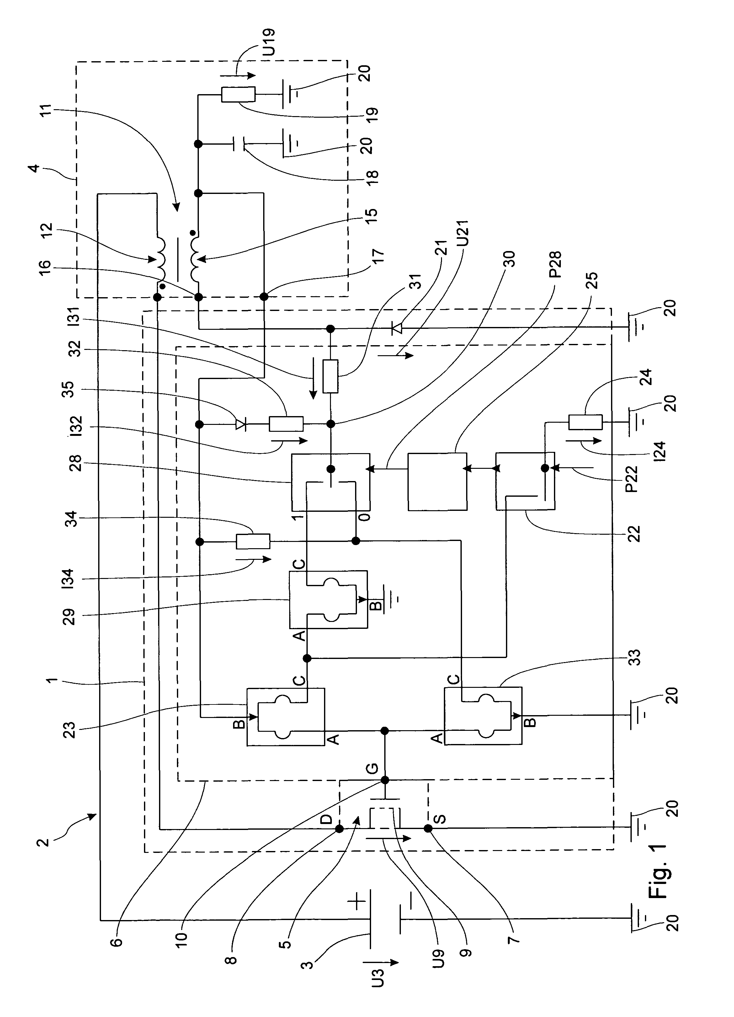
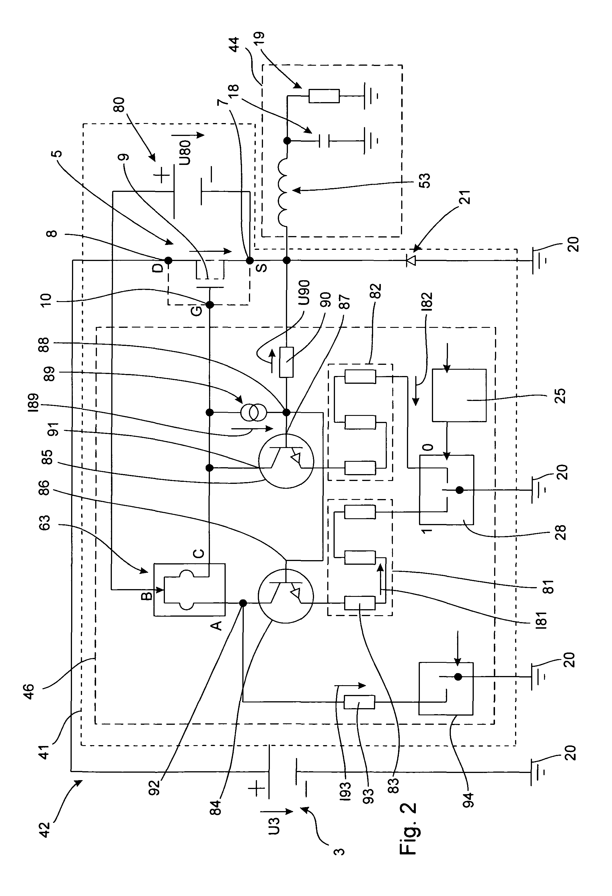
[0044]a control device 41 shown in FIG. 2 has substantially the same functionality as the control device 1, so that components with at least substantially the same function are provided with the same reference number.

first embodiment

[0045]By way of example, the load 44 has no transformer, as shown in the first embodiment according to FIG. 1, but instead includes a parallel connection of a capacitor 18 and a resistance 19, which are connected in series with an inductance 53. Both loads 4, 44 should in each case represent any desired combinations of electrical and / or electronic components with ohmic, inductive and capacitive elements.

[0046]Also connected in parallel to the load 44 in the second embodiment of the control device 41 are the freewheeling means in the form of the freewheeling diode 21. Alternatively, in both embodiments of the control circuit 6, 46, the freewheeling means may be in the form of a MOSFET, an IGBT or a SICFET.

[0047]Also provided for the control device 41, in addition to the voltage source 3, is an auxiliary voltage 80 with a supply potential U80 supplying power to the current mirror 63. If by way of example the semiconductor switch 5 is an NI-channel MOSFET, wired as source follower, the...


PUM


Abstract

A control device for influencing a flow of energy in a load circuit between an electrical voltage source and an electrical load, having a semiconductor switch including a conductive section which is formed between an input connection and an output connection, can be looped into the load circuit, and has an electrical resistance adjustable by means of an electrical potential which can be applied to a control connection associated with the semiconductor switch, and having a control circuit which is coupled to the control connection and includes a freewheeling means connected in parallel to the load. The control circuit is designed to supply a control current at the control connection which is proportional to a voltage via the freewheeling means.

Description

[0001]This application claims priority based on an International Application filed under the Patent Cooperation Treaty, PCT / EP2012 / 001932, filed May 4, 2012, which claims priority to DE102011100760.5, filed May 7, 2011.BACKGROUND OF THE INVENTION[0002]The invention relates to a control device for influencing a flow of energy in a load circuit between an electrical voltage source and an electrical load, having a semiconductor switch comprising a conductive section which is formed between an input connection and an output connection, which can be looped into the load circuit, and has an electrical resistance adjustable by means of an electrical potential which can be applied to a control connection associated with the semiconductor switch, and having a control circuit which is coupled to the control connection and comprises a freewheeling means, in particular a freewheeling diode, connected in parallel to the load. The invention also relates to a method for actuating a semiconductor s...

Claims


Application Information

Patent Timeline
IPC IPC(8): H03K3/00H02M1/44H03K17/082H03K17/16H03K17/28H03K17/284
CPCH03K17/16H02M1/44H03K17/166H03K17/082H03K17/28H03K17/0822H03K17/284
Inventor MARKS, WALTER
Owner MARKS WALTER
Why Eureka
Try Eureka