Display element, display device, and projection display device
a display element and display device technology, applied in the field of display elements, can solve the problems of improper directivity of light emitted, difficulty in narrowing the emission angle of light emitted from the display element to less than 15°, etc., and achieve the effect of high directivity and high luminan
- Summary
- Abstract
- Description
- Claims
- Application Information
AI Technical Summary
Benefits of technology
Problems solved by technology
Method used
Image
Examples
example 1
[0139]FIG. 12 shows an angle distribution of light that exits display element 1 according to the first embodiment. In FIG. 12, the horizontal axis represents the exit angle of light that exits display element 1, whereas the vertical axis represents the intensity thereof.
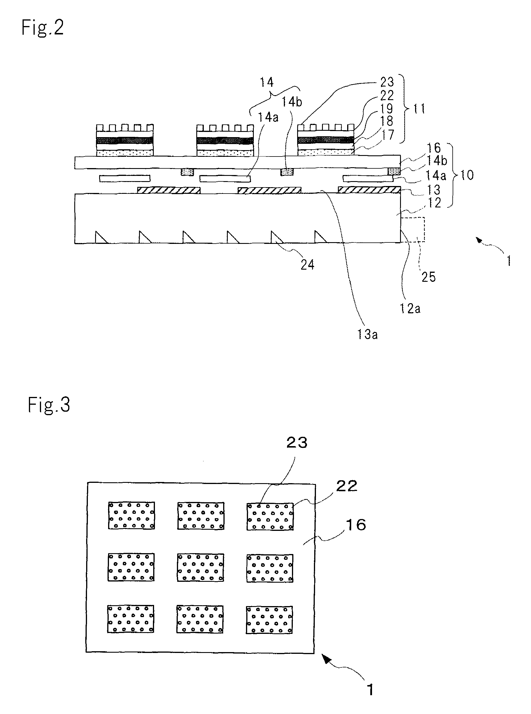
[0140]Substrate 16 made of SiO2, carrier generation layer 17 made of a fluorescent substance containing PVA (polyvinyl alcohol) as a primary component, first dielectric constant layer 18 made of porous SiO2, plasmon excitation layer 19 made of Ag, second dielectric constant layer 22 made of TiO2, and wave number vector conversion layer 23 made of TiO2 were prepared such that their thicknesses became 0.5 mm, 70 nm, 10 nm, 50 nm, 10 μm, and 950 nm, respectively. The wave length of light emitted from carrier generation layer 17 was 460 nm. The pitch and duty ratio of the periodic structure of wave number vector conversion layer 23 were set to 280 nm and 0.5, respectively. The dielectric constant of porous SiO2 was 1.12....
example 2
[0143]FIG. 13 shows an angle distribution of light emitted from display element 2 according to the second embodiment. In this example, calculations for the structure in which first dielectric constant layer 18 and second dielectric constant layer 22 were arranged in plasmon coupling sections 11 were performed. In FIG. 13, the horizontal axis represents the exit angle of light that exits display element 2, whereas the vertical axis represents the intensity thereof.
[0144]Substrate 16 made of SiO2, carrier excitation layer 17 made of a fluorescent substance containing PVA as a primary component, first dielectric constant layer 18 made of porous SiO2, plasmon excitation layer 19 made of Ag, second dielectric constant layer 22 made of Al2O3, and wave number vector conversion layer 23 made of PMMA (polymethyl methacrylate) were prepared such that their thicknesses became 0.5 mm, 100 nm, 10 nm, 50 nm, 10 nm, and 100 nm, respectively. The dielectric constant of porous SiO2 was 1.12. The dep...
PUM
| Property | Measurement | Unit |
|---|---|---|
| emission angle | aaaaa | aaaaa |
| dielectric constant | aaaaa | aaaaa |
| thickness | aaaaa | aaaaa |
Abstract
Description
Claims
Application Information
 - R&D
- Intellectual Property
- Life Sciences
- Materials
- Tech Scout
- Unparalleled Data Quality
- Higher Quality Content
- 60% Fewer Hallucinations
Browse by: Latest US Patents, China's latest patents, Technical Efficacy Thesaurus, Application Domain, Technology Topic, Popular Technical Reports.
© 2025 PatSnap. All rights reserved.Legal|Privacy policy|Modern Slavery Act Transparency Statement|Sitemap|About US| Contact US: help@patsnap.com


