System and method for photonically assisted analog to digital signal conversion

a technology of photon assisted analog and digital signal, applied in transmission systems, analogue/digital conversion, instruments, etc., can solve the problems of mainly limited, progress eventually slowed down, and difficulty in progress along either ax

Inactive Publication Date: 2015-02-24
YISSUM RES DEV CO OF THE HEBREWUNIVERSITY OF JERUSALEM LTD
View PDF15 Cites 3 Cited by
  • Summary
  • Abstract
  • Description
  • Claims
  • Application Information

AI Technical Summary

Benefits of technology

[0032]The present invention provides a novel photonically-assisted ADC technique, which is capable of improving either one or both of the main factors characterizing the ADC process, namely the sampling rate and the detection resolution. The ADC of the present invention can scale to operate at many sampling rates, for example 100 GS / s or faster, with improved quantization accuracy over the employed electrical ADC by way of signal processing applied to multiple samples of the same signal.
[0033]The ADC of the present invention is configured as internally-photonic structure but with electronic input / output interfaces. The role of photonics in the photonically-assisted ADC of the present invention is to first bridge the gap between electronic ADC abilities and sampling rate requirements, i.e. photonics is used as a serial to parallel converter of information by wavelength, and second to increase the accuracy of the conversion beyond the electrical ADC capabilities, i.e. photonics is used to oversample the information and reduce the error contributions by digital signal processing (DSP). The photonically-assisted ADC architecture of the present invention is based on converting the voltage-under-test (VUT) to phase modulation applied to an optical sampling pulse source or preferentially to a frame of sampling pulse distinguished by wavelength created by the technique of the invention or other known techniques. Operating under phase modulation provides greater linearity in the modulation response, and the present invention utilizes coherent detection concepts applied across multiple bases for quantizing the sampled information in shot-noise limited performance.
[0037]According to another aspect, the invention provides for high resolution conversion to digital procedure. The invention utilizes phase modulation of a clock signal (preferably a clock signal having the above described profile of ideal sampling pulse sequence) resulting from interaction of the clock signal with the input analog signal, followed by oversampling technique. The latter consists of interfering the modulated clock signal with a reference clock signal in a manner producing multiple interference samples. Collecting multiple samples of the interference pattern provides an increase in the measurements and by statistical error reduction means enables increased conversion resolution after processing all the samples jointly. Thus, the higher the number of interference samples, the higher is the sampling accuracy (resolution).
[0042]In some embodiments, the optical sampling signal generator comprises an optical dispersion compensator (TODC) having a spectral band narrower than that of a broadband short pulse spectrum, and a relatively wideband chromatic dispersive unit, to thereby provide spectrally and temporarily separate pulse train presenting a combined staircase group delay. The TODC may comprise one or more tunable chromatic dispersive elements, thereby being tunable in step height, the optical sampling signal generator thereby providing a tunable sampling frequency.
[0045]In some embodiments, the periodic dispersion unit comprises a dispersive assembly comprising an arrayed waveguide grating configured to form a phase array source, a spatial Fourier transformer, and a reflection-mode spatial light modulator, thereby enabling recombining of reflected and dispersed signals by back propagation through the same dispersive assembly, and being separated to an output fiber via a circulator. The periodic dispersion unit may further comprise a crossed diffraction grating dispersing light in a direction substantially perpendicular to a dispersion direction of the arrayed waveguide grating. Optionally, a half-wave plate may be further used to make the arrayed waveguide grating polarization-independent.

Problems solved by technology

While electronic ADC technology has vastly been improving, progress eventually slowed down.
Electronic ADC technology is the bottleneck today between high-speed analog signal acquisition and the accompanying digital signal processing.
Advance along either of these axes is extremely challenging and is mainly limited by the timing jitter of the electrical sampling circuitry.
It should be noted that the difficulty of attaining high vertical resolution grows extremely rapidly with frequency.
Adding ENOBs is an exponentially difficult task, as each extra ENOB means quadrupling the overall SNR from all noise sources.

Method used


Image

  • System and method for photonically assisted analog to digital signal conversion
  • System and method for photonically assisted analog to digital signal conversion
  • System and method for photonically assisted analog to digital signal conversion

Examples


Embodiment Construction

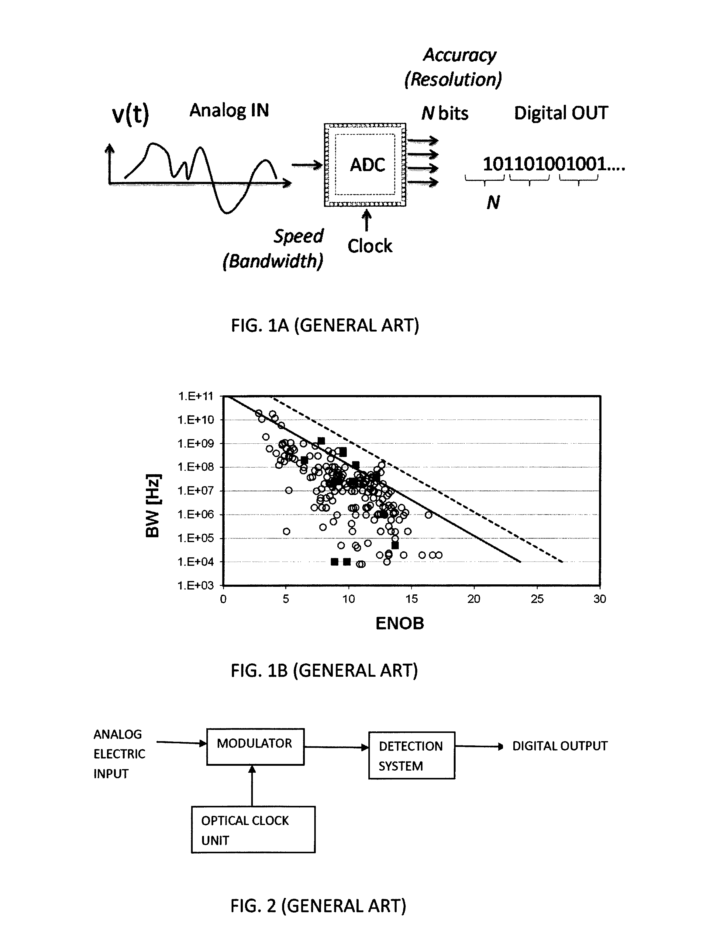
[0062]FIG. 1A schematically illustrates the principles of electronic ADC technology, and FIG. 1B illustrates the state of the art ADC technology at the time of submission. FIG. 2 shows a typical photonic ADC system.

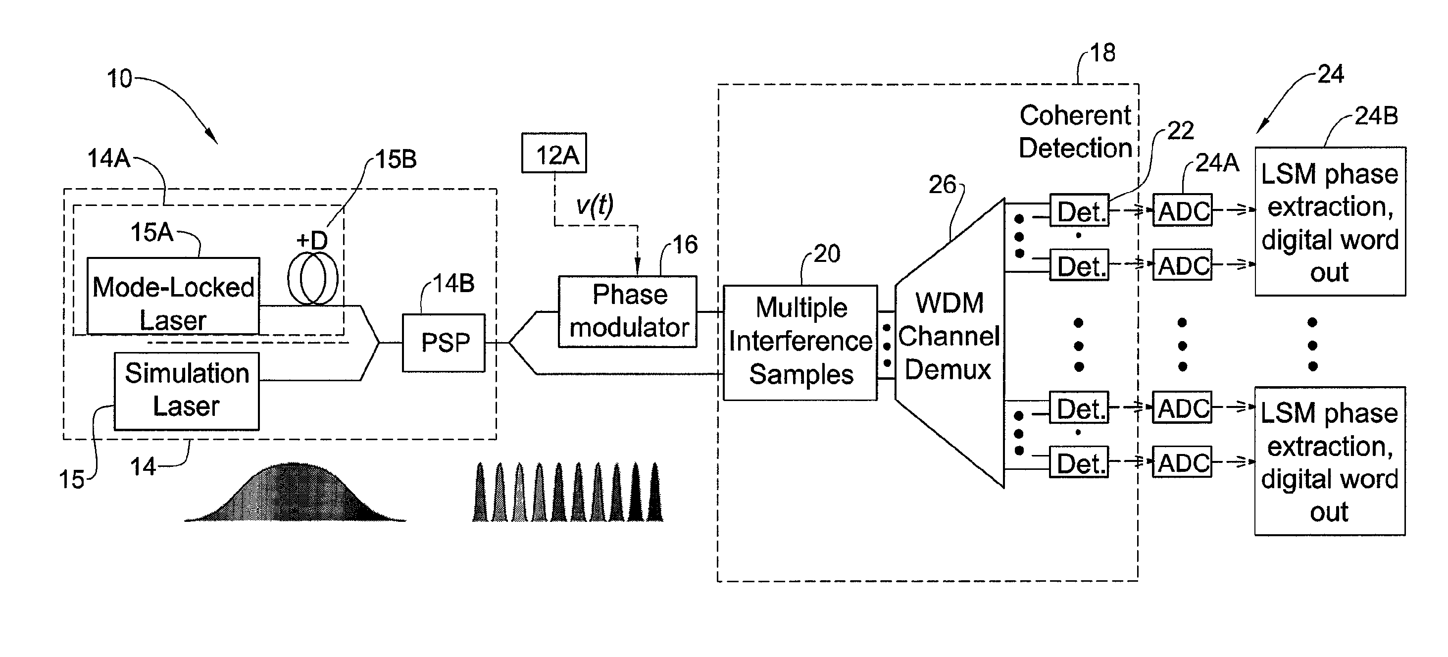
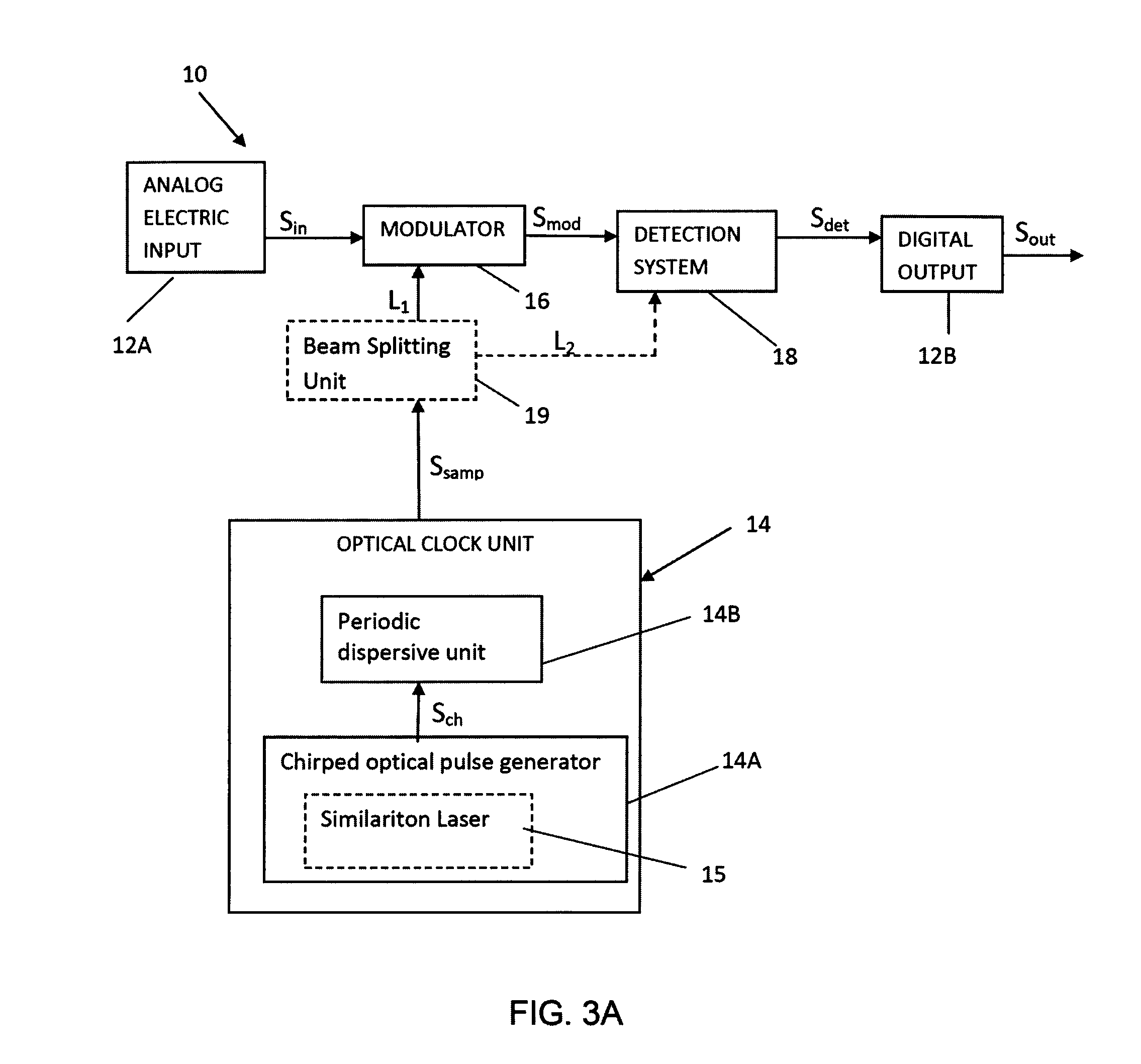
[0063]Reference is made to FIGS. 3A to 3D showing four examples, respectively, of a photonically-assisted ADC system of the present invention. To facilitate understanding, the same reference numbers are used for identifying those components which are common in all the examples of the invention.

[0064]A system of the present invention, generally designated 10, is configured as internally-photonic structure but with electronic input / output interfaces, and includes the following main functional components: input and output ports 12A and 12B for inputting analog electric input Sin and outputting digital electric output Sout; an optical sampling signal generator (optical clock unit) 14, modulator 16 and detection system 18. Optical clock unit 14 is configured for producing a sa...


PUM

PropertyMeasurementUnit
focal lengthaaaaaaaaaa
central wavelengthaaaaaaaaaa
phaseaaaaaaaaaa

Abstract

A photonically assisted analog to digital conversion (ADC) system is presented. The system comprises: an optical sampling signal generator configured and operable for generating an optical sampling signal comprising a predetermined sampling pulse sequence in the form of a time separated pulse train of spectral components dispersed in a periodic fashion, where each pulse is distinguishable by a central wavelength thereof different from its neighboring pulses. The generation of the pulse sampling sequence is achieved by combining broadband dispersion and compensation with a periodic dispersion compensator having a free spectral range smaller than the broad bandwidth of the ultrashort pulse. The second innovative element is the introduction of coherent detection with oversampling of the interference terms of the phase modulated pulse sampling sequence and a reference pulse. The over-sampling provides additional measurements of the beat term and by way of error minimization a more reliable phase estimation is provided, translated into a more accurate conversion to digital representation. The system further comprises an electro-optical modulator for interacting an input electric analog signal and an optical sampling signal and generating a modulated optical signal indicative of said input signal; and a detection system configured and operable for receiving said modulated optical signal and generating an output digital signal corresponding to said input electric analog signal.

Description

FIELD OF THE INVENTION[0001]This invention is generally in the field of analog to digital signal conversion, and relates to a system and method for photonically assisted analog to digital signal conversion.REFERENCES[0002]The following references are considered to be pertinent for the purpose of understanding the background of the present invention:[0003]1. Y. M. Greshishchev et al., “A 40 GS / s 6b ADC in 65 nm CMOS,” Solid-State Circuits Conference Digest of Technical Papers (ISSCC), 2010 IEEE International, 390-391, 7-11 Feb. 2010[0004]2. M. El-Chammas and B. Murmann, “A 12-GS / s 81-mW 5-bit Time-Interleaved Flash ADC with Background Timing Skew Calibration,” 2010 IEEE Symposium on VLSI Circuits, Honolulu, Hi., June 2010.[0005]3. G. C. Valley, Photonic analog-to-digital converters, Opt. Express, 15, 1955-1982 (2007).[0006]4. R. C. Williamson, P. W. Juodawlkis, J. L. Wasserman, G. E. Betts, and J. C. Twichell, “Effects of crosstalk in demultiplexers for photonic analog-to-digital con...

Claims


Application Information

Patent Timeline
Patent Type & Authority Patents(United States)
IPC IPC(8): H03M1/12G02F7/00
CPCH03M1/1205G02F7/00H03M1/1245H03M1/124
Inventor MAROM, DAN MARK
Owner YISSUM RES DEV CO OF THE HEBREWUNIVERSITY OF JERUSALEM LTD
Why Eureka
Try Eureka