
Layout decomposition method and apparatus for multiple patterning lithography

a patterning lithography and decomposition method technology, applied in the field of semiconductor integrated circuit design and manufacture, can solve the problems of significant difficulties in the practical implementation of these euv processes, increasing the difficulty of circuit features and other layout shapes formed using conventional single pattern lithography processes, and difficulty in overlay control

Inactive Publication Date: 2014-08-05
INT BUSINESS MASCH CORP
View PDF5 Cites 9 Cited by
  • Summary
  • Abstract
  • Description
  • Claims
  • Application Information

AI Technical Summary

Benefits of technology

[0008]Illustrative embodiments of the present invention provide improved techniques for decomposing an integrated circuit design layout into multiple sub-layouts suitable for use in a multiple patterning lithography process.
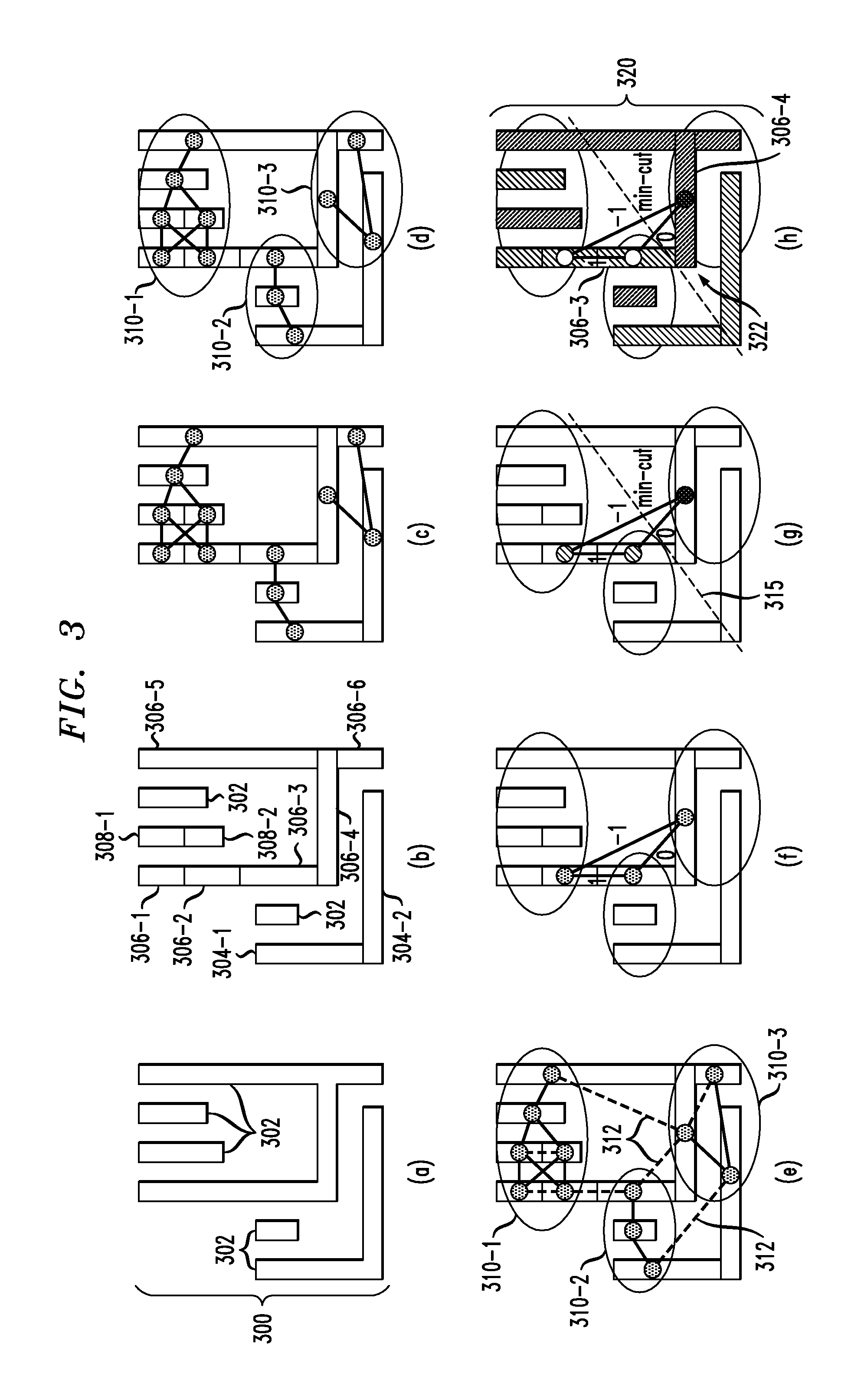
[0011]One or more of the illustrative embodiments advantageously provide optimal minimization in the number of stitches between the segments of the multiple sub-layouts, while also providing a substantially reduced complexity which is given generally by O(n1.5 log n), where n denotes the number of segments in the layout after separation of each of its shapes into one or more segments. Using the techniques disclosed herein, the problem of minimizing the number of stitches, which is believed to be NP-hard using conventional ILP approaches, can be reduced to a min-cut problem on a planar graph, resulting in a highly efficient decomposition process that is even faster than conventional heuristics approaches.

Problems solved by technology

As integrated circuit device dimensions continue to shrink, it is becoming increasingly difficult to form circuit features and other layout shapes using conventional single pattern lithography processes.
The recent development of extreme ultra violet (EUV) single pattern lithography processes will potentially allow the accurate patterning of ultra deep submicron shapes, but there remain significant difficulties in the practical implementation of these EUV processes.
Such overlay control is particularly challenging in view of rounding errors that typically arise at the ends of actual printed shapes at the stitch locations due to the lithography process, and the difficulty of the overlay control increases with the number of stitches.
However, obtaining optimal decompositions using the ILP approaches is unduly complex and time-consuming, and therefore such approaches are generally not suitable for use with layouts that include very large numbers of circuit features and other shapes.
The heuristics approaches are also problematic in that such approaches tend to result in sub-optimal decompositions, that is, decompositions in which the number of stitches is not minimized.

Method used


Image

  • Layout decomposition method and apparatus for multiple patterning lithography
  • Layout decomposition method and apparatus for multiple patterning lithography
  • Layout decomposition method and apparatus for multiple patterning lithography

Examples


Embodiment Construction

[0017]The present invention will be illustrated herein in conjunction with exemplary integrated circuit design systems and associated techniques for generating circuit layouts. It should be understood, however, that the invention is not limited to use with the particular types of systems and techniques disclosed. The invention can be implemented in a wide variety of other types of design systems, using alternative circuit layout generation techniques. For example, although illustrated herein primarily in the context of DPT techniques, which generally involve decomposing a given layout into first and second sub-layouts, the disclosed arrangements can be adapted in a straightforward manner for use with other types of multiple patterning lithography processes, including those involving decomposition into three or more sub-layers.

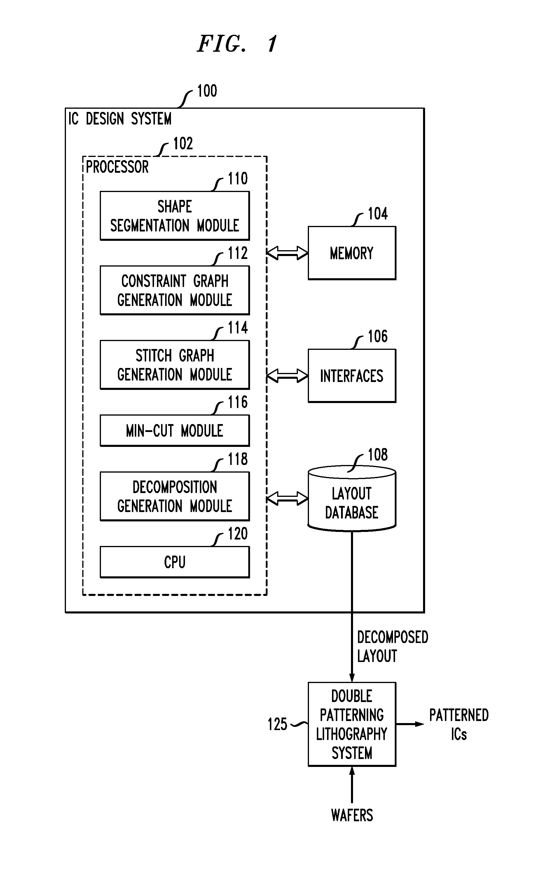
[0018]FIG. 1 shows an integrated circuit (IC) design system 100 in an illustrative embodiment of the invention. The system comprises a processor 102, which is ...


PUM


Abstract

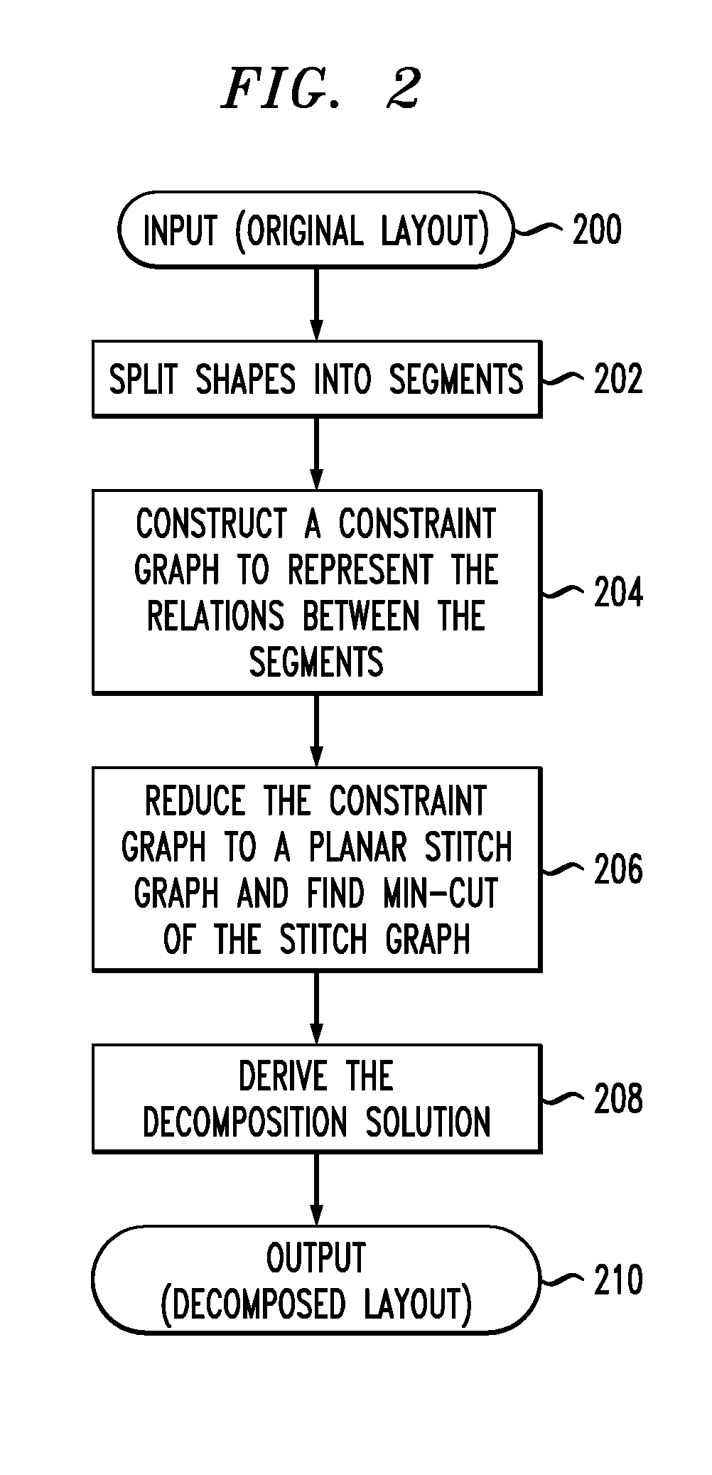
An initial layout of at least a portion of a given layer of an integrated circuit design is decomposed into multiple sub-layouts by splitting each of a plurality of shapes of the initial layout into multiple segments, constructing a constraint graph to represent relationships between the segments, reducing the constraint graph to a stitch graph, determining at least one cut line of the stitch graph, and generating a decomposed layout based on the determined cut line. The decomposed layout in an illustrative embodiment includes first and second sub-layouts comprising respective disjoint subsets of the segments, with each of the sub-layouts of the decomposed layout being associated with a different pattern mask of a double patterning lithography process. The layout decomposition process advantageously minimizes the number of stitches between the sub-layouts without introducing excessive computational complexity.

Description

FIELD OF THE INVENTION[0001]The present invention relates generally to semiconductor integrated circuit design and manufacture, and more particularly to techniques for generating circuit layouts in an integrated circuit design process.BACKGROUND OF THE INVENTION[0002]As integrated circuit device dimensions continue to shrink, it is becoming increasingly difficult to form circuit features and other layout shapes using conventional single pattern lithography processes. The recent development of extreme ultra violet (EUV) single pattern lithography processes will potentially allow the accurate patterning of ultra deep submicron shapes, but there remain significant difficulties in the practical implementation of these EUV processes.[0003]An alternative approach to extending the range of conventional lithography processes is known as double patterning technology (DPT). The DPT approach generally involves decomposing the layout of a given layer of an integrated circuit design into two sep...

Claims


Application Information

Patent Timeline
Patent Type & Authority Patents(United States)
IPC IPC(8): G06F17/50
CPCG03F1/68G03F1/70G03F7/70433G03F7/70475
Inventor CHO, MINSIKTANG, XIAOPING
Owner INT BUSINESS MASCH CORP
Learn More