
Monolithic ceramic electronic component including outer-layer dummy electrode groups

a technology of monolithic ceramic and electronic components, applied in the direction of fixed capacitor details, stacked capacitors, fixed capacitors, etc., can solve the problems of difficult forming of outer electrodes with high accuracy, limited accuracy of applying thick film paste, and general deformation so as to reduce the degradation of reliability of monolithic ceramic electronic components, reduce the distance between inner electrodes, and shorten the distance

Active Publication Date: 2014-08-05
MURATA MFG CO LTD
View PDF29 Cites 10 Cited by
  • Summary
  • Abstract
  • Description
  • Claims
  • Application Information

AI Technical Summary

Benefits of technology

The invention relates to a method for improving the reliability of monolithic ceramic electronic components. The method involves arranging two or more outer-layer dummy conductors at predetermined intervals to ensure proper plating deposition points and relieve pressing of inner electrodes. The distance between inner electrodes is prevented from being locally shortened, which can lead to reduced reliability. The preferred embodiment of the invention sets the interval between adjacent outer-layer dummy groups to be longer to allow for continuous formation of the plated film for the first outer electrode.

Problems solved by technology

Hence characteristics of the monolithic ceramic electronic component generally tend to degrade.
However, a known method of baking a thick film paste has a limit in accuracy of applying the paste and has a difficulty in forming the outer electrodes with high accuracy.
With the method disclosed in Japanese Unexamined Patent Application Publication No. 2004-327983, however, reliability, e.g., breakdown voltage or BDV, of the monolithic ceramic electronic component may degrade in some cases.
As a result, the inventors have discovered that the degradation of reliability (BDV) is attributable to the presence of the dummy conductors.

Method used


Image

  • Monolithic ceramic electronic component including outer-layer dummy electrode groups
  • Monolithic ceramic electronic component including outer-layer dummy electrode groups
  • Monolithic ceramic electronic component including outer-layer dummy electrode groups

Examples


first preferred embodiment

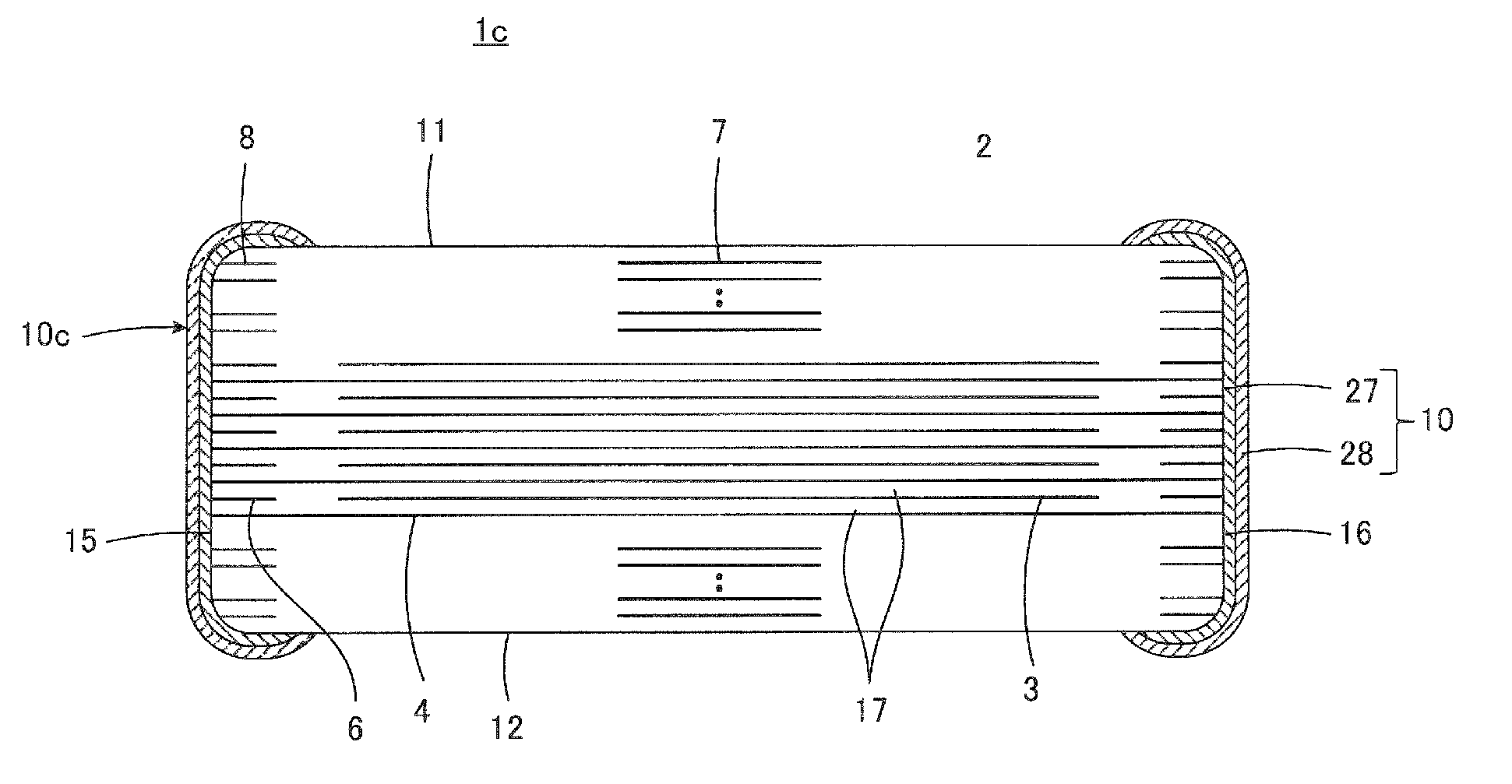
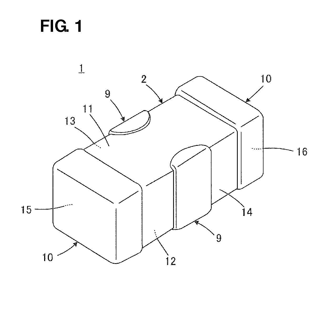
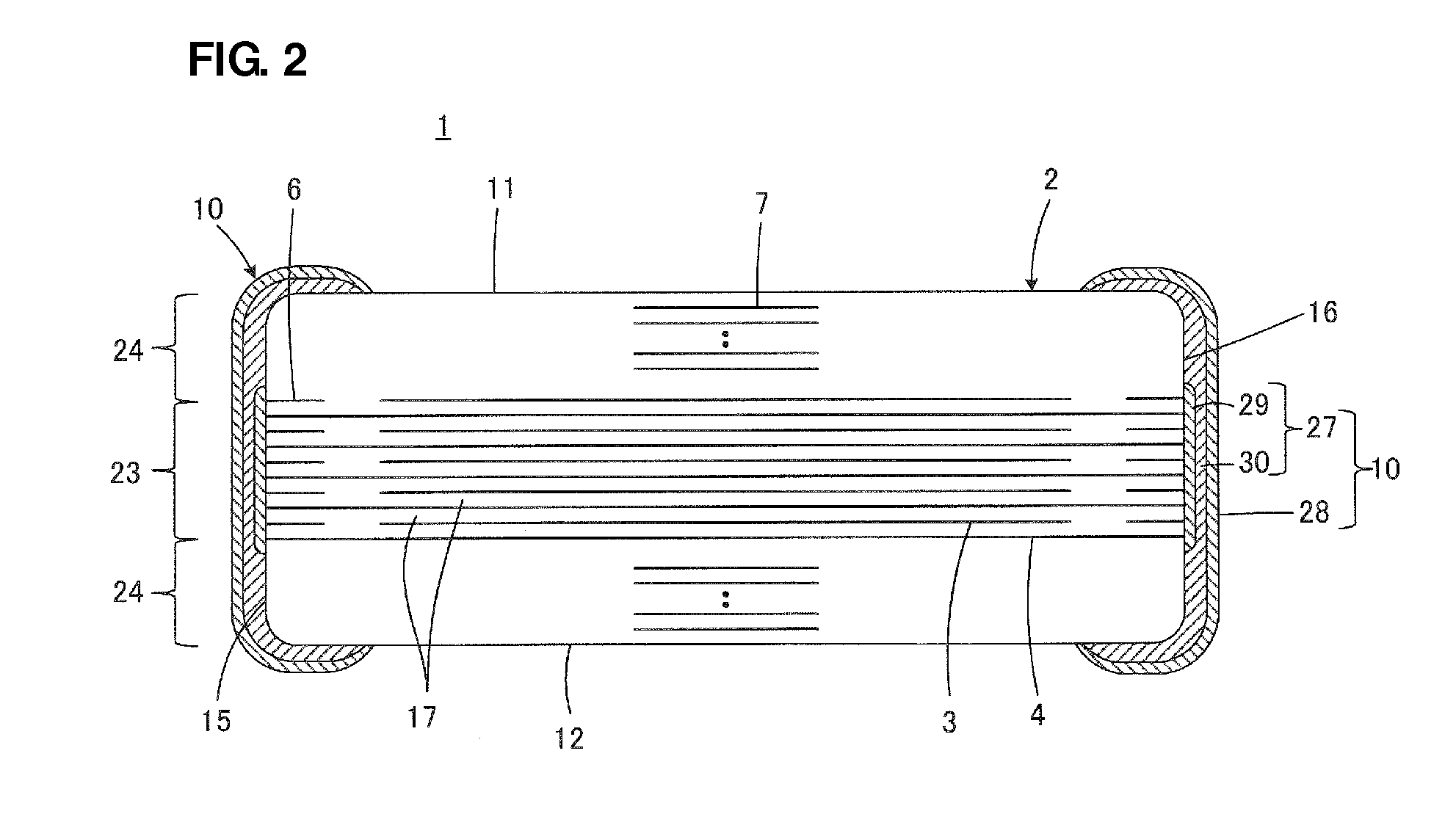
[0034]A first preferred embodiment of the present invention will be described below with reference to FIGS. 1 to 7. A monolithic ceramic capacitor 1 according to the first preferred embodiment preferably is of the three-terminal type, for example. The monolithic ceramic capacitor 1 includes a ceramic base element 2. The monolithic ceramic capacitor 1 further includes first and second inner electrodes 3 and 4, first and second inner-layer dummy conductors 5 and 6, and outer-layer dummy conductors 7, which are all disposed inside the ceramic base element 2, as well as first and second outer electrodes 9 and 10, which are disposed on outer surfaces of the ceramic base element 2. Details of the structure of the monolithic ceramic capacitor 1 will be described below in order of (1) Ceramic Base Element, (2) Inner Electrode, (3) Inner-Layer Dummy Conductor, (4) Outer-Layer Dummy Conductor, and (5) Outer Electrode. Description of (6) manufacturing method follows thereafter.

(1) Ceramic Base...

second preferred embodiment

[0099]A second preferred embodiment of the present invention is illustrated in FIG. 8. FIG. 8 is a sectional view corresponding to FIG. 3. Equivalent elements in FIG. 8 to those in FIG. 3 are denoted by the same reference symbols and duplicate descriptions of those elements are omitted here.

[0100]In a monolithic ceramic capacitor 1a according to the second preferred embodiment, an outer-layer dummy conductor 7a is arranged such that the outer-layer dummy conductor 7a does not penetrate through the ceramic base element 2 in the widthwise direction and it is separated in the widthwise direction.

third preferred embodiment

[0101]A third preferred embodiment of the present invention is illustrated in FIGS. 9 and 10. FIG. 9 is a perspective view corresponding to FIG. 1, and FIG. 10 is a sectional view corresponding to FIG. 3. Equivalent elements in FIGS. 9 and 10 to those in FIGS. 1 and 3 are denoted by the same reference symbols and duplicate descriptions of those elements are omitted here.

[0102]A monolithic ceramic capacitor 1b according to the third preferred embodiment includes a first outer electrode 9b, including an underlying layer 25 and an overlying layer 26 thereof, arranged to extend over the first and second lateral surfaces 13 and 14 and the first and second principal surfaces 11 and 12 of the ceramic base element 2 in a fully surrounding state.

[0103]In this preferred embodiment, the outer-layer dummy conductors 7 are preferably exposed in at least respective portions of the principal surfaces 11 and 12 by chipping off the ceramic layers 17, which define the principal surfaces 11 and 12, in...


PUM

PropertyMeasurementUnit
thicknessaaaaaaaaaa
thicknessaaaaaaaaaa
distanceaaaaaaaaaa

Abstract

Two or more outer-layer dummy conductors are successively arranged at predetermined intervals in the height direction, thereby forming a plurality of outer-layer dummy groups. Given that an interval between the adjacent outer-layer dummy conductors within each of the outer-layer dummy groups is d and an interval between the adjacent outer-layer dummy groups is g, g is greater than d. On that condition, the outer-layer dummy groups can be positioned satisfactorily apart away from each other, while plating deposition points are ensured. As a result, pressing of inner electrodes through the outer-layer dummy conductors can be relieved, whereby the distance between the inner electrodes can be prevented from being locally shortened and a reduction of BDV can be prevented.

Description

BACKGROUND OF THE INVENTION[0001]1. Field of the Invention[0002]The present invention relates to a monolithic ceramic electronic component, and more particularly to a monolithic ceramic electronic component provided with outer electrodes including plated films that are directly disposed on outer surfaces of a ceramic base element.[0003]2. Description of the Related Art[0004]Recently, sizes of electronic devices, such as cellular phones, notebook personal computers, digital cameras, and digital audio devices, have become increasingly smaller. Monolithic ceramic electronic components capable of being manufactured to have smaller sizes but with higher performance have been used in many of such electronic devices.[0005]The monolithic ceramic electronic component usually includes a ceramic base element including a plurality of stacked ceramic layers, inner electrodes formed inside the ceramic base element, and outer electrodes formed on outer surfaces of the ceramic base element. Further...

Claims


Application Information

Patent Timeline
Patent Type & Authority Patents(United States)
IPC IPC(8): H01G4/005H01G4/06H01L41/047H01L41/273H01L41/29
CPCH01L41/0471H01L41/273H01L41/29H10N30/871H10N30/053H10N30/06H01G4/30H01G4/12
Inventor SAKURATANI, MASAHIROYAMAMOTO, SHIGEKATSU
Owner MURATA MFG CO LTD
Learn More