Substrate and substrate bonding device using the same

a technology of substrate and bonding device, which is applied in the direction of insulated conductors, flat/ribbon cables, cables, etc., can solve the problems of substrate detachment, poor contact, and weak bonding strength between two substrates, so as to avoid substrate detachment and poor contact, avoid the effect of bonding area and bonding strength

Active Publication Date: 2014-07-15
AU OPTRONICS CORP
View PDF33 Cites 2 Cited by
  • Summary
  • Abstract
  • Description
  • Claims
  • Application Information

AI Technical Summary

Benefits of technology

[0008]The invention is directed to a substrate and a substrate bonding device using the same. Through the design of double- or multi-layered metal layer of the substrate, the bonding area between the substrate and another substrate is increased, so that the bonding strength between two substrates is increased, and problems such as substrate detachment and poor contact are avoided.
[0009]According to a first aspect of the present invention, a substrate connected to another substrate is provided. The another substrate has two bonding portions which are insulated with each other. The substrate includes a base, a lower metal layer, a lower covering layer, an upper metal layer and an upper covering layer. The base has an upper surface, a lower surface, and a through hole which passes through the upper surface and the lower surface. The lower metal layer is disposed on the lower surface of the base, and has an electrical bonding portion and a strengthening bonding portion which are insulated with each other. The strengthening bonding portion is used for enhancing the bonding strength between the substrate and the another substrate. The lower covering layer covers the lower metal layer and exposes the electrical bonding portion and the strengthening bonding portion, so that the electrical bonding portion and the strengthening bonding portion are respectively bonded with two bonding portions of the another substrate. The upper metal layer is disposed on the upper surface of the base and electrically connected to the electrical bonding portion via the through hole. The upper covering layer covers the upper metal layer.
[0010]According to a second aspect of the present invention, a substrate bonding device including a first substrate and a second substrate is provided. The first substrate has a first electrical bonding portion and a first strengthening bonding portion which are insulated with each other. The second substrate includes a base, a lower metal layer, a lower covering layer, an upper metal layer, and an upper covering layer. The base has an upper surface, a lower surface, and a through hole passing through the upper surface and the lower surface. The lower metal layer is disposed on the lower surface of the base, and has a second electrical bonding portion and a second strengthening bonding portion which are insulated with each other. The lower covering layer covers the lower metal layer and exposes the second electrical bonding portion and the second strengthening bonding portion, so that the second electrical bonding portion and the second strengthening bonding portion are bonded with the first electrical bonding portion and the first strengthening bonding portion respectively. The upper metal layer is disposed on the upper surface of the base, and electrically connected to the second electrical bonding portion via the through hole. The upper covering layer covers the upper metal layer. The first and the second strengthening bonding portions are bonded with each other for enhancing the bonding strength between the first substrate and the second substrate.

Problems solved by technology

However, the bonding area of the bonding portion 14 is restricted by the layout spaces of the electronic elements on the substrate, so that the bonding strength between two substrates is too weak to resist the pulling force during the assembly process.
As a consequence, problems such as substrate detachment and poor contact may occur easily.

Method used


Image

  • Substrate and substrate bonding device using the same
  • Substrate and substrate bonding device using the same
  • Substrate and substrate bonding device using the same

Examples


first embodiment

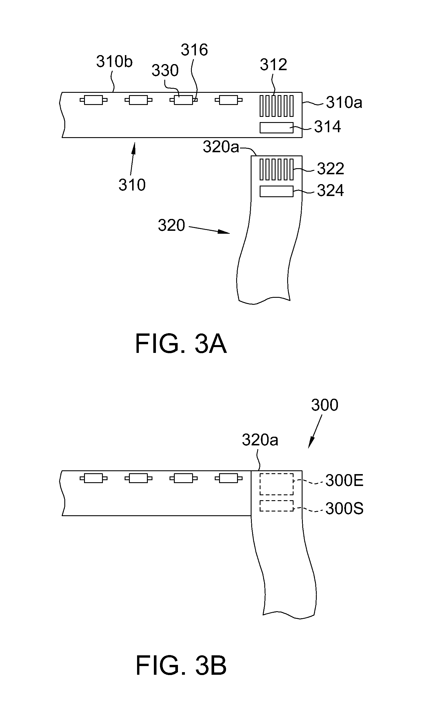
[0022]Referring to FIGS. 3A and 3B, two diagrams of a substrate bonding device according to a first embodiment of the invention are shown. The substrate bonding device 300 includes a first substrate 310 and a second substrate 320. The first substrate 310 can be realized by a rigid substrate, and the second substrate 320 can be realized by a flexible substrate. As indicated in FIG. 3A, the first substrate 310 has a first electrical bonding portion 312 and a first strengthening bonding portion 314 which are insulated with each other, and the second substrate 320 has a second electrical bonding portion 322 and a second strengthening bonding portion 324 which are insulated with each other.

[0023]Note that, the second substrate 320 of the present embodiment of the invention can be realized by the substrate 200 of FIG. 2 which has a double- or a multi-layered metal structure. The first substrate 310 of the present embodiment of the invention can be realized by the substrate 100 of FIG. 2 w...

second embodiment

[0027]Referring to FIGS. 4A and 4B, two diagram of a substrate bonding device according to a second embodiment of the invention are shown. The substrate bonding device 400 of the present embodiment of the invention is different from the substrate bonding device 300 of the first embodiment in the bonding position between the first substrate and the second substrate, and other features similar to the first embodiment are not repeated here. In FIG. 4A, the first substrate 410 has two opposite long sides 410b to which the first electrical bonding portion 412 and the first strengthening bonding portion 414 are adjacent respectively. Besides, the second substrate 420 has an edge 420a to which the second electrical bonding portion 422 and the second strengthening bonding portion 424 are adjacent, wherein the second electrical bonding portion 422 is located between the edge 420a and the second strengthening bonding portion 424. The first substrate 410 is preferably a light bar, and further ...

third embodiment

[0030]Referring to FIGS. 5A and 5B, two diagrams of a substrate bonding device according to a third embodiment of the invention are shown. The substrate bonding device 500 of the present embodiment of the invention is different from the substrate bonding device 300 of the first embodiment in the substrate type of the first substrate, and other features similar to the first embodiment are not repeated here. The substrate bonding device 500 includes a first substrate 510 and a second substrate 520. The first substrate 510 and the second substrate 520 can both be realized by a flexible substrate.

[0031]The second electrical bonding portion 522 and the second strengthening bonding portion 524 of the second substrate 520 of FIG. 5A are respectively bonded with the first electrical bonding portion 512 and the first strengthening bonding portion 514 of the first substrate 510 of FIG. 5A to form a substrate bonding device 500 of FIG. 5B. The first and the second electrical bonding portion 51...


PUM

PropertyMeasurementUnit
bonding strengthaaaaaaaaaa
electricalaaaaaaaaaa
flexibleaaaaaaaaaa

Abstract

A substrate and a substrate bonding device using the same are provided. The substrate includes a base, upper and lower metal layers, and upper and lower covering layers. The base has an upper surface, a lower surface and a through-hole passing there through, wherein the upper and lower covering layers respectively covers the upper and lower metal layers respectively disposed on the upper and lower surfaces of the base. The lower metal layer has an electrical bonding portion and a strengthening bonding portion insulated with each other. The strengthening bonding portion enhances the bonding strength between the substrate and another substrate. The upper metal layer is electrically connected to the electrical bonding portion via the through hole. The lower covering layer exposes the electrical bonding portion and the strengthening bonding portion so as to be respectively connected with two bonding portions of the another substrate.

Description

[0001]This application claims the benefit of Taiwan application Serial No. 98145941, filed Dec. 30, 2009, the subject matter of which is incorporated herein by reference.BACKGROUND OF THE INVENTION[0002]1. Field of the Invention[0003]The invention relates in general to a substrate and a substrate bonding device using the same, and more particularly to a substrate with at least double-layered metal layer and a substrate bonding device using the same.[0004]2. Description of the Related Art[0005]The printed circuit board (PCB) is a supporter of electronic elements and provides the connection of wires between the electronic elements. The base of the PCB can be phenolic sheets, glass fabric sheets or various plastic sheets. For example, the base of the FR-4 substrate is formed by epoxy glass fabric sheets.[0006]The flexible printed circuit (FPC) is light, thin, soft and flexible, and has been widely used in many electronic products such as mobile phones, notebook computers, PDAs, digital...

Claims


Application Information

Patent Timeline
Patent Type & Authority Patents(United States)
IPC IPC(8): H01R4/00H01B7/08H02G3/06H02G15/08H05K1/00
CPCH01R12/62B23K1/0016B23K2201/38H01R4/021H01R13/58B23K2101/38
Inventor WANG, CHUNG-CHUANHUANG, CHI-HSIANGHSU, TZU-HUI
Owner AU OPTRONICS CORP
Why Eureka
Try Eureka