Data bus inversion using spare error correction bits

a data bus and error correction technology, applied in the field of computer system memory, can solve the problems of reducing the voltage margin between the signal voltage and the signal voltage, affecting the signal voltage, and the noise is typically presen

Active Publication Date: 2014-03-18
LENOVO GLOBAL TECH INT LTD
View PDF20 Cites 12 Cited by
  • Summary
  • Abstract
  • Description
  • Claims
  • Application Information

AI Technical Summary

Problems solved by technology

Some amount of noise is typically present in the channel, which affects the signal voltage.
However, reducing the signal voltage also reduces the voltage margin between the signal voltage and the reference voltage with which the signal is compared.
If the magnitude of the fixed reference voltage is not suitable, then the available voltage margin may be inadequate and result in reduced signal reliability.
Double Data Rate (DDR) memory is susceptible to noise problems, such as Inter Symbol Interference (ISI) and Simultaneous Switching Output (SSO) noise, which can cause reduced voltage margins and corrupted data.
Such noise problems may be caused, in part, by package, connector, and circuit board parasitics.
The power consumption of a memory system is also affected by bus switching, which is the alternating voltages in the bus signal line changes as the voltage levels between values of 0 and 1.

Method used


Image

  • Data bus inversion using spare error correction bits
  • Data bus inversion using spare error correction bits
  • Data bus inversion using spare error correction bits

Examples


Embodiment Construction

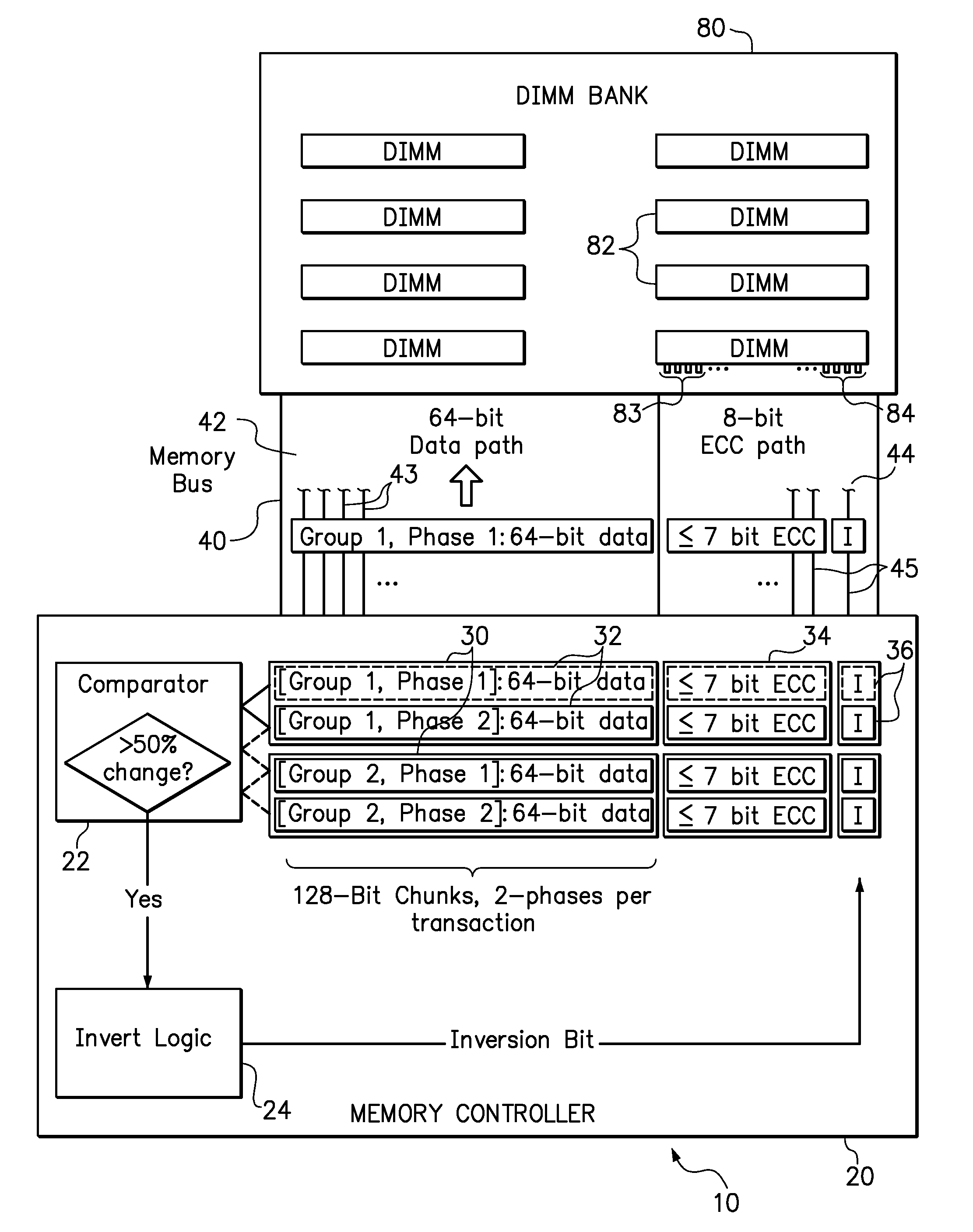
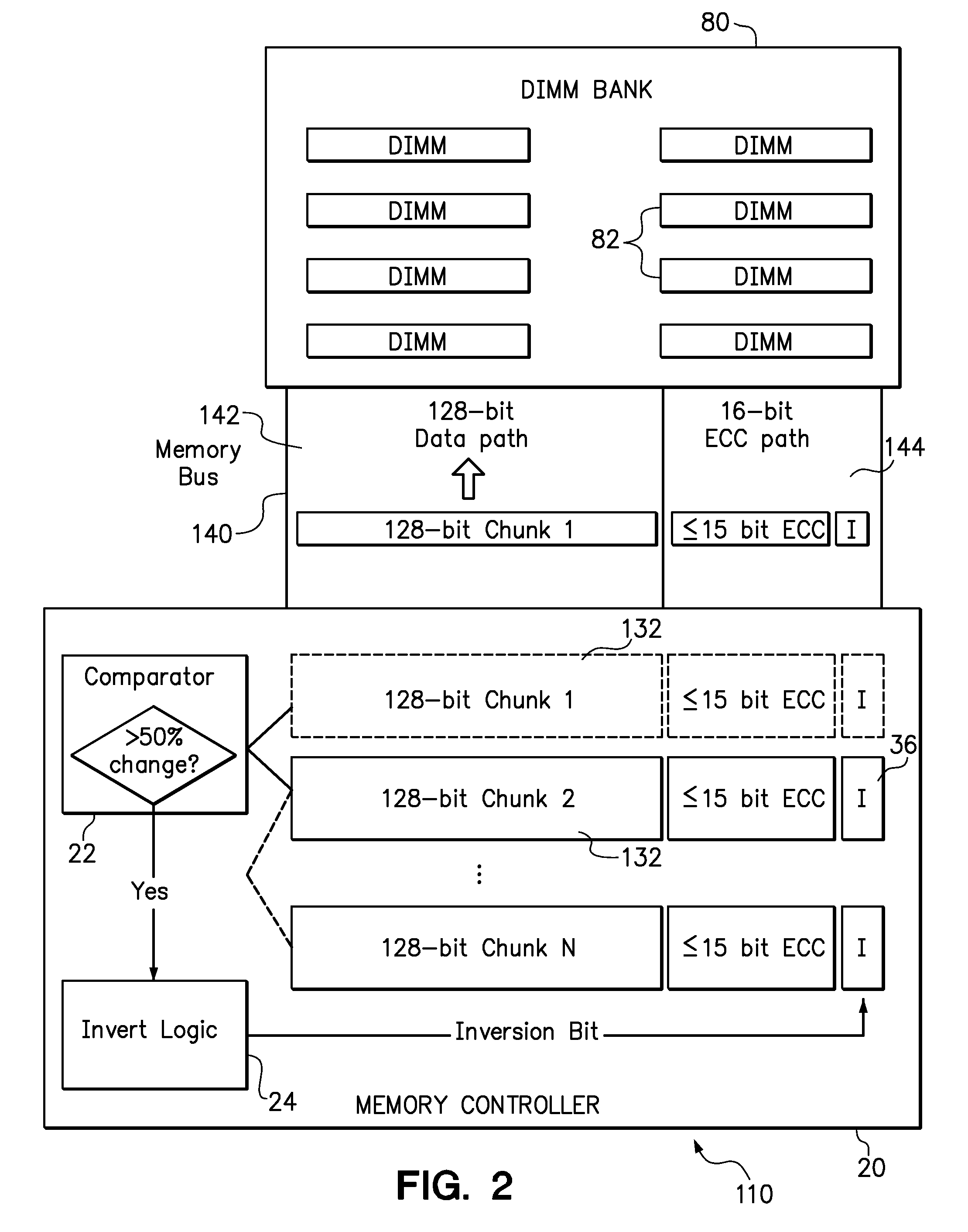
[0015]Embodiments of the invention include systems and methods for implementing parallel data bus inversion using standard, unmodified memory module and bus components. In a conventional error correction scheme, such as Hamming Single Error Correct, Double Error Detect (SECDED), the number of error correction (“ECC”) bits required to protect a portion of data does not increase linearly with the number of data bits in that portion. For example, an error correction scheme that requires 8 ECC bits to protect a 64-bit chunk of memory data may require fewer than 16 ECC bits to protect a 128-bit chunk of data. Therefore, one of the disclosed features is to generate “spare” bits by transmitting memory on a memory bus using sufficiently large chunk of data that proportionally fewer ECC bits are required. The “spare bits” refer to both to signal lines in the memory bus and memory cells in the memory modules that are normally allocated to the transmission and storage of ECC bits. These spare ...


PUM


Abstract

In a memory system, a spare error correction bit is produced by processing data to be stored in sufficiently large chunks that the number of error correction bits required to protect each chunk are fewer than the available error correction signal lines on a memory bus and storage device. The spare bit is then used for an inversion bit in a parallel data bus inversion scheme, wherein data is selectively inverted to minimize bus switching. The transmission of data and error correction bits are spread over multiple phases, wherein parallel data bus inversion is applied to each phase. Alternatively, the transmission of data and error correction bits may be transmitted and stored in a single transaction. In either case, the spare bit is transmitted on a conventional memory bus and stored in a conventional memory module along with data and error correction bits.

Description

BACKGROUND[0001]1. Field of the Invention[0002]The present invention relates to computer system memory, and in particular to systems and methods for implementing parallel data bus inversion.[0003]2. Background of the Related Art[0004]Digital memory systems store information in binary form using logical 0s and 1s. A digital memory system includes a driver to generate time-dependent voltage signals that represent the different logic levels. The logic levels are interpreted at a receiver according to the voltage values received. The voltage of a signal may be compared with a reference voltage at the receiver to determine which logic states are being represented at each instance of a clock signal. The reliability of the signal is dependent on the voltage margin between the signal and the reference voltage. Some amount of noise is typically present in the channel, which affects the signal voltage.[0005]As computer technology advances, processor speeds continue to increase, creating a dem...

Claims


Application Information

Patent Timeline
Patent Type & Authority Patents(United States)
IPC IPC(8): G11C29/00
CPCG06F11/1048
Inventor BANDHOLZ, JUSTIN, P.
Owner LENOVO GLOBAL TECH INT LTD
Why Eureka
Try Eureka