TCAD emulation calibration method of SOI field effect transistor

a field effect transistor and calibration method technology, applied in semiconductor/solid-state device testing/measurement, instrumentation, program control, etc., can solve the problems of large deviation between the simulation device structure and the actual structure, large error in emulation electrical parameters, and complicated manufacturing process and device structure characteristics, etc., to achieve accurate and effective pre-test and effective guidance

Inactive Publication Date: 2014-03-04
SHANGHAI INST OF MICROSYSTEM & INFORMATION TECH CHINESE ACAD OF SCI
View PDF5 Cites 0 Cited by
  • Summary
  • Abstract
  • Description
  • Claims
  • Application Information

AI Technical Summary

Benefits of technology

[0025]in the TCAD emulation calibration method provided in the present invention, TCAD emulation model parameters are reasonably and effectively calibrated by using actual test data such as TEM and SIMS results, a CV test curve, and a WAT test, so that in the same SOI process, TCAD emulation results of key parameters Vt and Idsat of MOSFETs of different sizes all meet a high-precision requirement that an error is less than 10%; moreover, accurate and effective pretest can be implemented in the case of multiple splits, thereby providing effective guidance for research, development and optimization of a new process flow.

Problems solved by technology

However, with the continuous reduction of IC feature size, the IC manufacturing process and the device structure characteristics tend to be more and more complex.
In an actual application of TCAD emulation, an emulation result is usually distorted resulting in deviation between simulation device structure and an actual structure and a great error in emulation electrical parameters.
The cases all greatly affect reliability and precision of TCAD emulation, so that a TCAD emulation result cannot provide effective guidance for an actual process and device research and development.

Method used


Image

  • TCAD emulation calibration method of SOI field effect transistor
  • TCAD emulation calibration method of SOI field effect transistor
  • TCAD emulation calibration method of SOI field effect transistor

Examples


Embodiment Construction

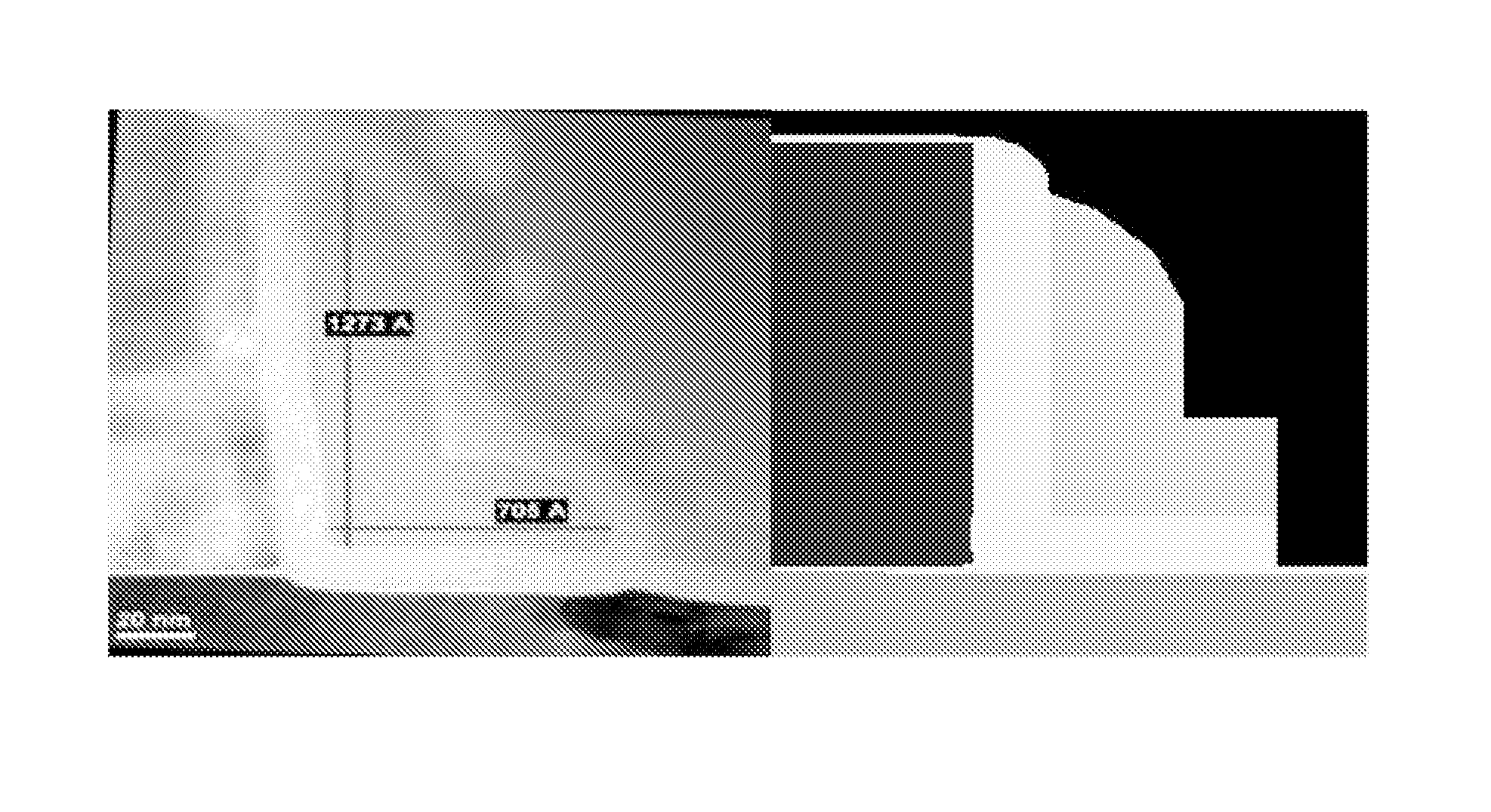
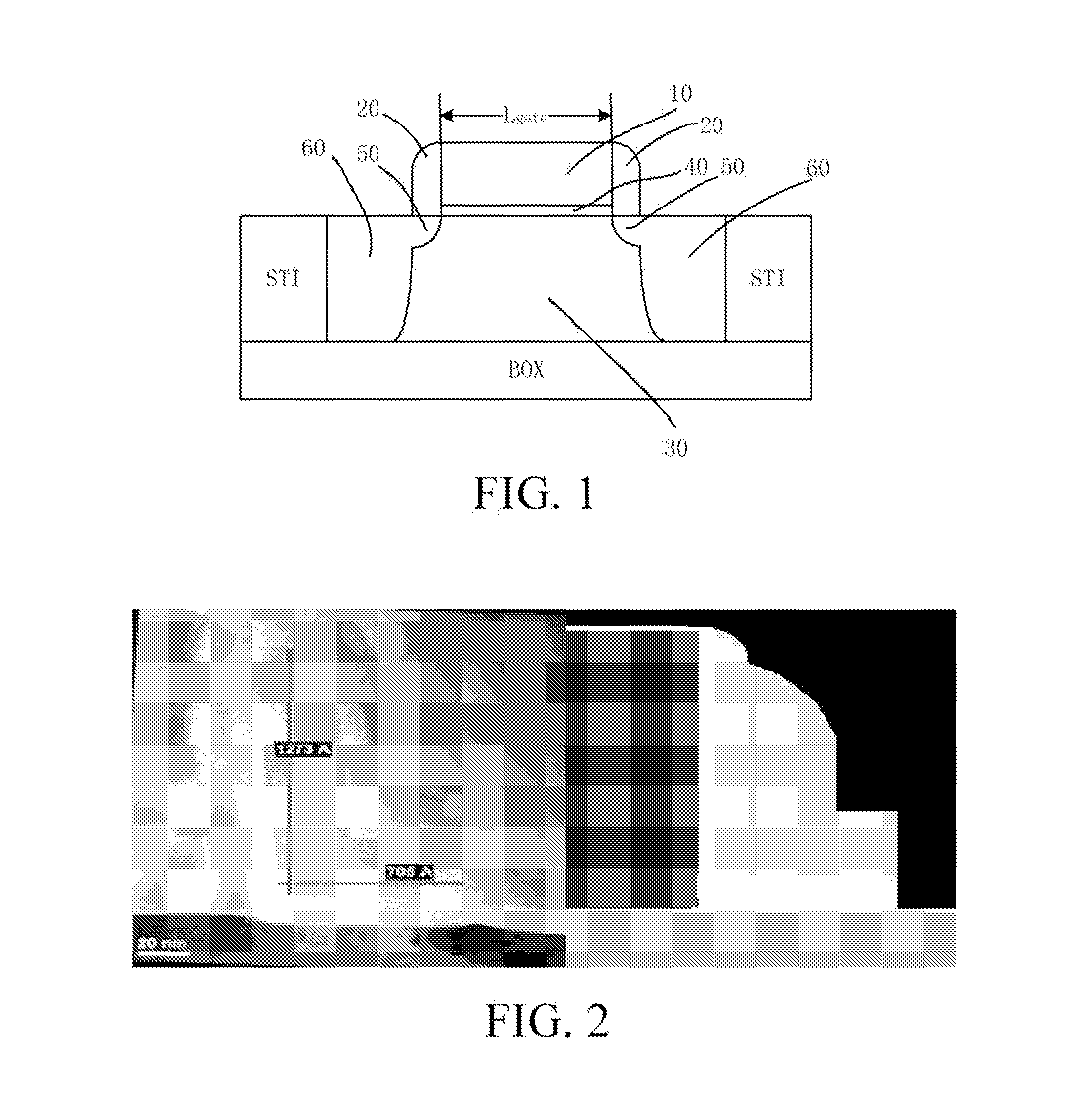
[0031]A TCAD calibration method consistent with the present invention is further described in the following with reference to the accompanying drawings.

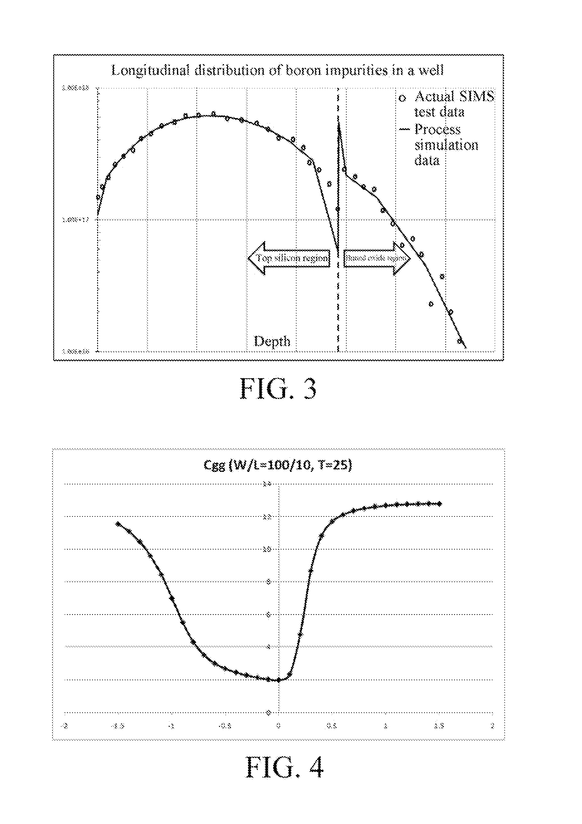
[0032]The inventor of the present invention performs error analysis on a preliminary TCAD emulation result of an SOI field effect transistor, and find through research that, in comparison with WAT test data, for key electrical parameters, threshold voltages Vt and saturation currents Idsat, of MOS devices with different channel lengths, a great error occurring in the TCAD emulation result mainly results from deviations of injected impurity distribution of the well in the process emulation, injected impurity distribution of an S / D slightly doped extending region, injected impurity distribution of an S / D region, a shape of a sidewall spacer, and a thickness Tox value of a gate oxide layer in the device emulation. The injected impurity distribution of the well and the thickness Tox value of the gate oxide layer in the device emulation a...


PUM


Abstract

A calibration method for a device using TCAD to emulation SOI field effect transistor, where process emulation MOS device structures with different channel lengths Lgate are obtained by establishing a TCAD process emulation program; the process emulation MOS device structures are calibrated according to a TEM test result, a SIMS test result, a CV test result, a WAT test result, and a square resistance test result of an actual device, so as to complete TCAD emulation calibration of key electrical parameters of an SOI field effect transistor. Thereby, providing effective guidance for research, development and optimization of a new process flow are realized.

Description

CROSS REFERENCE TO RELATED PATENT APPLICATION[0001]The present application is the US national stage of PCT / CN2011 / 080076 filed on Sep. 23, 2011, which claims the priority of the Chinese patent application No. 201110112178.1 filed on May 3, 2011, which application is incorporated herein by reference.BACKGROUND OF THE PRESENT INVENTION[0002]1. Field of Invention[0003]The present invention relates to semiconductor device emulation technologies, and specifically to a Technology Computer Aided Design (TCAD) emulation calibration method of a Silicon On Insulator (SOI) field effect transistor, belonging to the field of micro-electronic devices.[0004]2. Description of Related Arts[0005]TCAD of an Integrated Circuit (IC) process and IC device technology is an important component of design and virtual manufacturing of an IC device, and is a powerful tool of rapidly analyzing characteristics of the IC process and device. IC TCAD mainly includes process emulation and device emulation. The proce...

Claims


Application Information

Patent Timeline
Patent Type & Authority Patents(United States)
IPC IPC(8): G06F17/50G06F9/455
CPCG06F17/5036H01L22/20G06F17/5081G06F30/367G06F30/398
Inventor CHAI, ZHANCHEN, JINGLUO, JIEXINWU, QINGQINGWANG, XI
Owner SHANGHAI INST OF MICROSYSTEM & INFORMATION TECH CHINESE ACAD OF SCI
Why Eureka
Try Eureka