Light-emitting display device and method for manufacturing the same
a technology of light-emitting display and manufacturing method, which is applied in the direction of semiconductor devices, organic semiconductor devices, electrical apparatus, etc., can solve the problems of reducing the yield of light-emitting display devices, limiting the thickness reduction of such substrates, and reducing the electric characteristics of thin film transistors. , to achieve the effect of reducing the number of photomasks
- Summary
- Abstract
- Description
- Claims
- Application Information
AI Technical Summary
Benefits of technology
Problems solved by technology
Method used
Image

Examples
embodiment 1
(Embodiment 1)
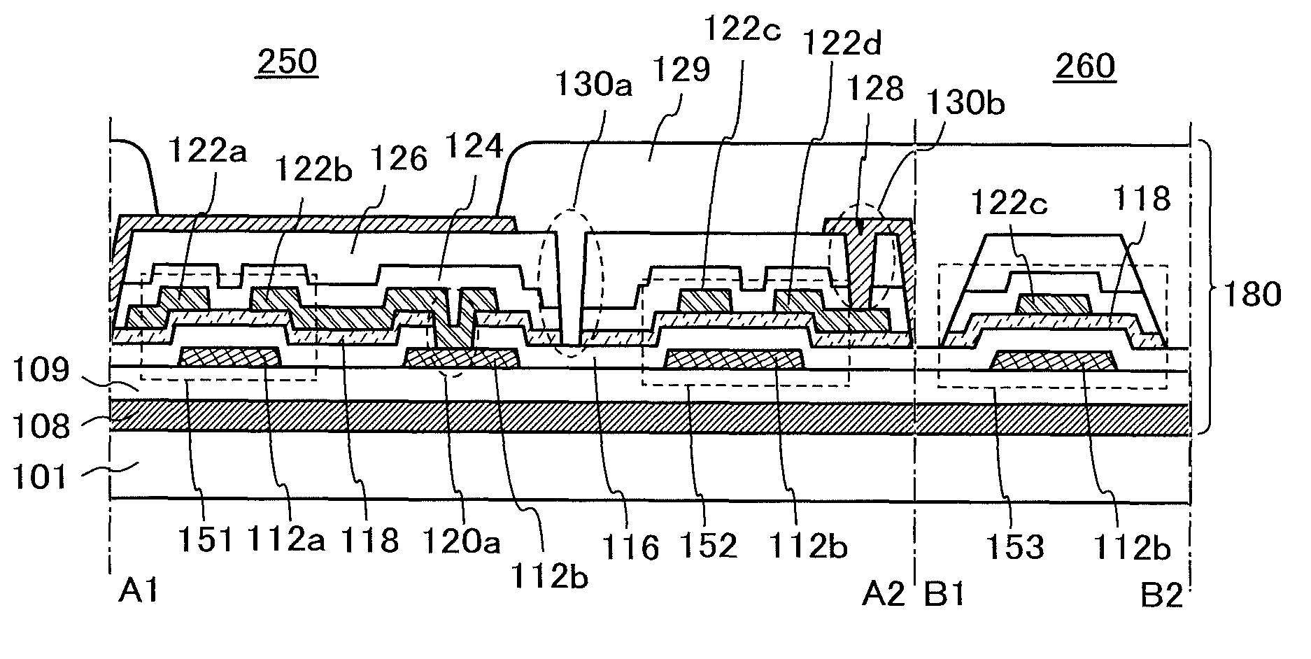
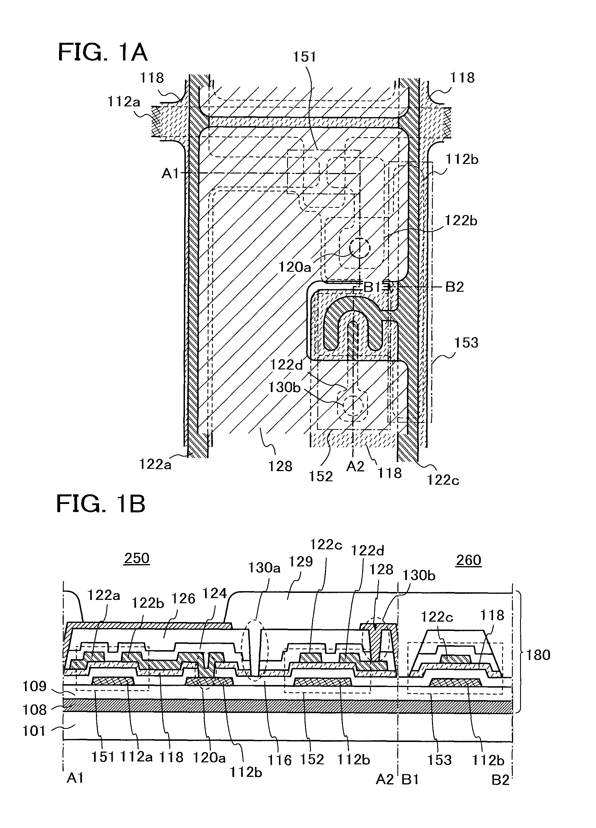
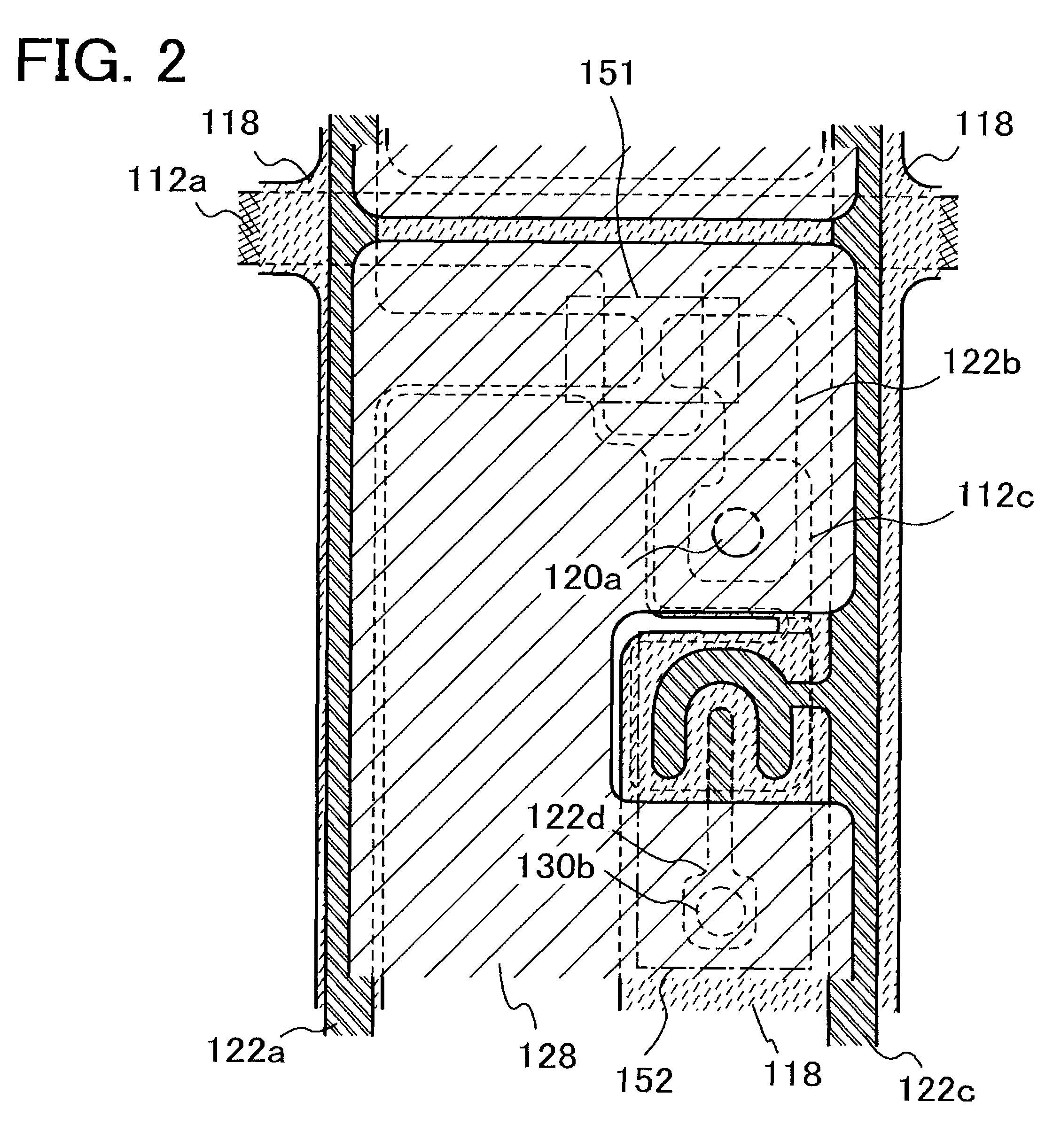
[0061]In this embodiment, a structural example of a pixel portion included in a light-emitting display device according to one embodiment of the present invention will be described with reference to FIGS. 1A and 1B, FIG. 2, FIG. 3, and FIGS. 4A and 4B. Note that description will be made in this embodiment assuming that the structure of the pixel portion is a top emission structure; however, an embodiment of the present invention is not limited thereto. As general emission structures other than a top emission structure, a bottom emission structure, a dual emission structure, and the like are given. Since those skilled in the art know these structures well, specific description of such emission structures is omitted in this embodiment.
[0062]FIG. 3 shows a structure example of a semiconductor device 100 used in a light-emitting display device. The semiconductor device 100 includes, over a substrate 101, a pixel region 102 provided with a plurality of pixels 110, a termina...
embodiment 2
(Embodiment 2)
[0203]In this embodiment, a process example partly different from that described in Embodiment 1 is described with reference to FIGS. 9A to 9C. Note that in FIGS. 9A to 9C, the same reference numerals are used for the same parts as those in FIGS. 5A to 5C, and specific description of the parts with the same reference numerals is omitted here. Further this embodiment is only partly different from Embodiment 1; thus, description is made focusing on only the structure of the transistor 151.
[0204]First, as in Embodiment 1, the separation layer 108 is formed over the substrate 101 having an insulating surface, the base layer 109 is formed over the separation layer 108, and a first conductive layer is formed over the base layer 109, a first resist mask is formed over the first conductive layer, and then, the first conductive layer is partly etched using the first resist mask to form the first gate electrode 112a.
[0205]In this embodiment, the base layer 109 has a function of...
embodiment 3
(Embodiment 3)
[0216]In this embodiment, an example of a structure of a light-emitting display device which is thin, lightweight, and significantly tough and which is manufactured in such a manner that the element region 180 formed in Embodiments 1 and 2 is separated from the substrate 101 and is provided over a different support will be described with reference to FIGS. 10A and 10B. In addition, an example of a method for manufacturing the light-emitting display device will be described with reference to FIGS. 11A and 11B, FIGS. 12A and 12B, and FIGS. 13A and 13B.
[0217]Note that as a display element included in the light-emitting display device, a light-emitting element utilizing electroluminescence is used here. Light-emitting elements utilizing electroluminescence are classified according to whether a light-emitting material is an organic compound or an inorganic compound. In general, the former is referred to as an organic EL element, and the latter is referred to as an inorganic...
PUM
 Abstract
Description
Claims
Application Information
 - R&D
- Intellectual Property
- Life Sciences
- Materials
- Tech Scout
- Unparalleled Data Quality
- Higher Quality Content
- 60% Fewer Hallucinations
Browse by: Latest US Patents, China's latest patents, Technical Efficacy Thesaurus, Application Domain, Technology Topic, Popular Technical Reports.
© 2025 PatSnap. All rights reserved.Legal|Privacy policy|Modern Slavery Act Transparency Statement|Sitemap|About US| Contact US: help@patsnap.com