Surface mount bias tee

Active Publication Date: 2014-02-04
SCI COMPONENTS
View PDF15 Cites 14 Cited by
  • Summary
  • Abstract
  • Description
  • Claims
  • Application Information

AI Technical Summary

Benefits of technology

The present invention is a surface mount bias tee that is more cost-effective and has better performance than previous designs. It consists of a printed circuit board with two pairs of body bonding pads where the first body is bonded to one pair of pads and the second body is bonded to the other pair. An inductor with a wire coil is positioned atop the first and second bodies, and two wire ends are conductively bonded to the pads. The second body, which is a non-circuit component, acts as a spacer for positioning the inductor. The two first body bonding pads, along with the inductor bonding pad, are connected to pads on the bottom face of the circuit board, which reduces parasitic inductance and extends the operating frequency range of the bias tee. The bias tee can be held and moved using surface mount pick and place machinery. The invention provides a miniature bias tee that has a flat frequency performance and is free from resonance over a range of at least 10 MHz to 10 GHz and from -40 degrees Celsius to -85 degrees Celsius.

Problems solved by technology

Further, manufacturing this bias tee requires multiple layers of LTCC to be custom made, assembled and then fused, which requires very specialized manufacturing equipment.
Additionally, a second inductor is required, further increasing part and assembly cost.
A major challenge is to vertically stack components without incurring excessive cost.
However, this stacking methodology lends itself best to uniformly sized rectangular components, but poorly to the sort of wound coil inductors best suited for high frequency signals.

Method used


Image

  • Surface mount bias tee
  • Surface mount bias tee
  • Surface mount bias tee

Examples


Embodiment Construction

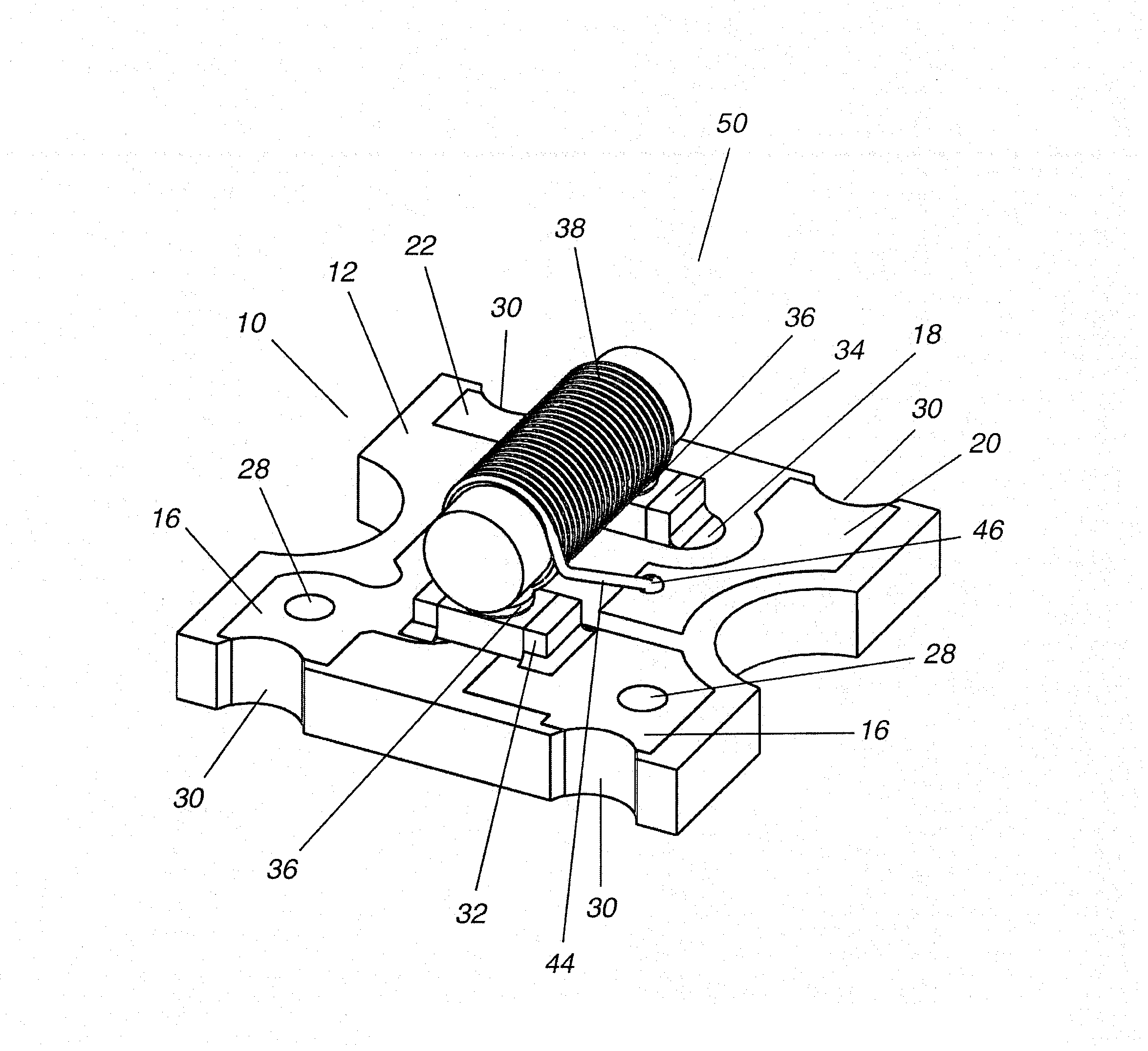
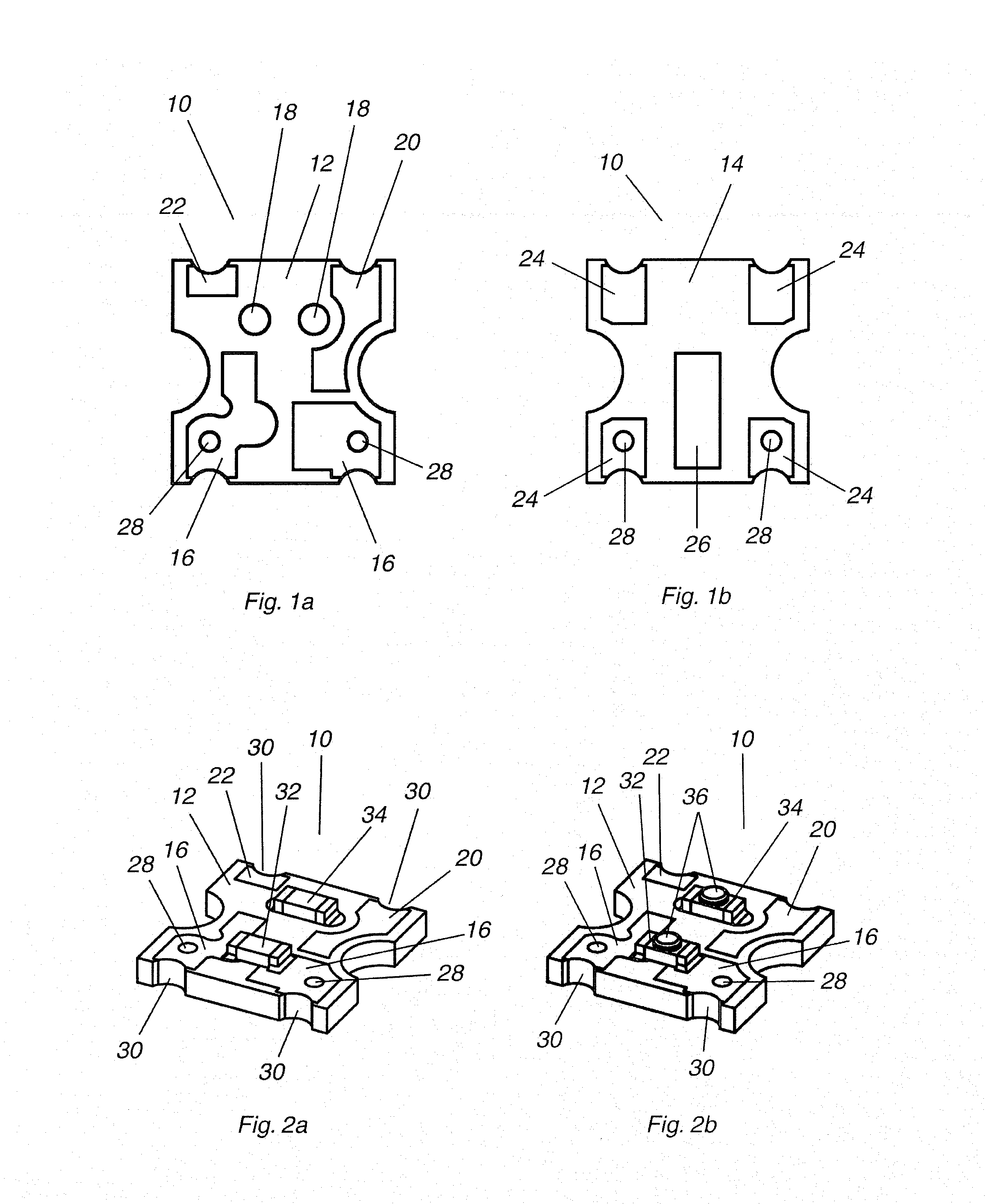
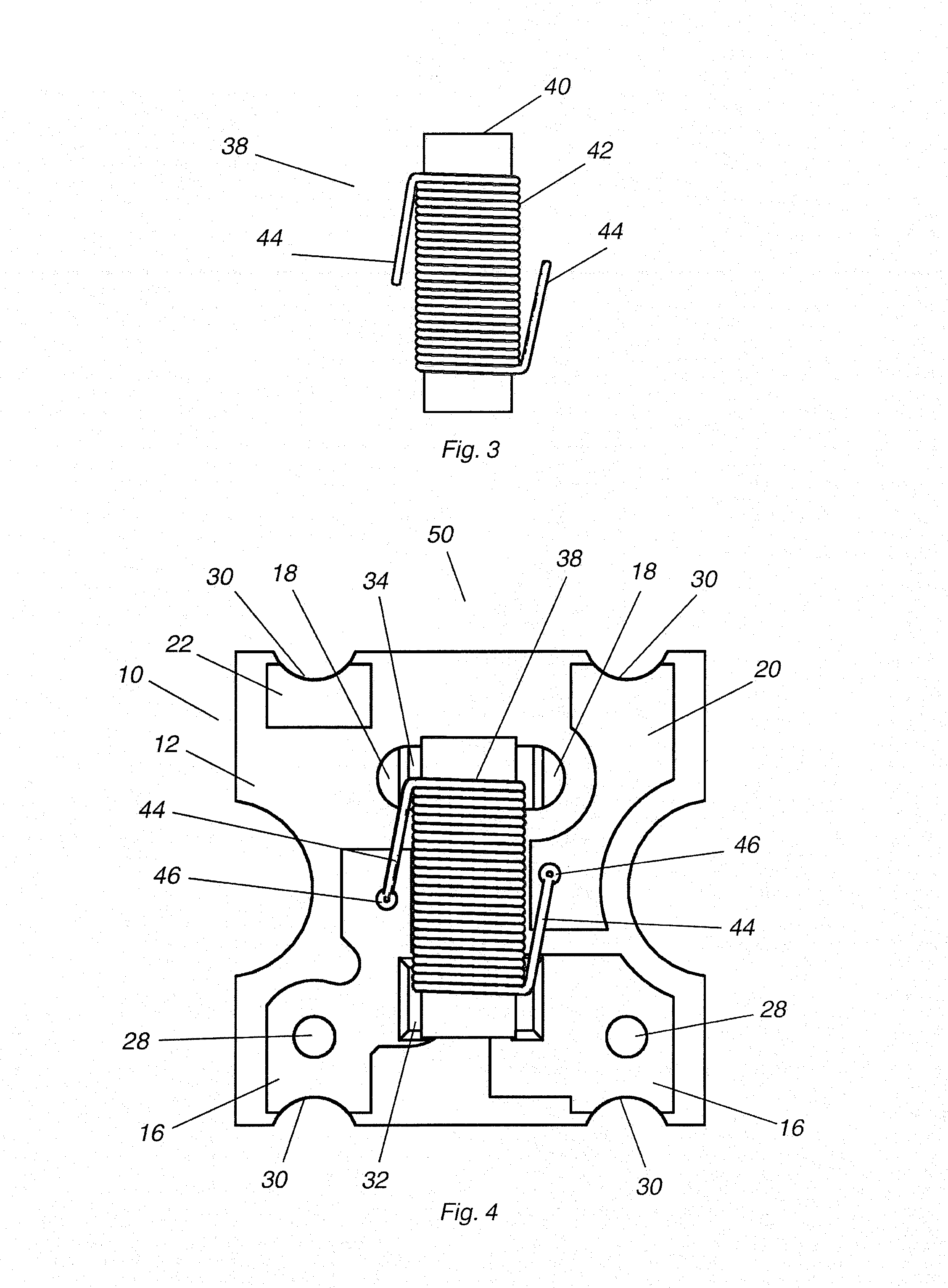
[0030]As shown in FIGS. 1a and 1b, a printed circuit board 10 has component bonding pads on a top face 12. These pads are used to bond several components or bodies, which for the first component or body is a capacitor and for the second component or body may be a spacer element designed for interchangeability with the first body, or may be a second capacitor which in this circumstance is a noncircuit element functioning as a spacer. The component bonding pads include a pair of first body bonding pads 16, a pair of second body bonding pads 18, an inductor bonding pad 20, and an open bonding pad 22. The bottom face 14 has four bottom bonding pads 24 and a bonding pad which is preferably treated as a ground pad 26. Four notches with edge metallization 30 provide conductive signal paths between the bonding pads on the top face 12 and the bonding pads on the bottom face 14. The notches are a preferred feature serving to reduce the chances of the component tombstoning (tipping on end) dur...


PUM


Abstract

A miniaturized wideband surface mount bias tee comprises a printed circuit board with a functioning first capacitor and a dummy second capacitor, and an inductor bonded atop the two capacitors. The capacitors, adhesive and solder are depositable by standard surface mount pick and place machinery. The inductor wires are bonded to one of the first capacitor bonding pads and to an inductor bonding pad. The circuit element bonding pads include portions bordering the pc board edges and are conductively connected to bonding pads on the bottom face of the pc board. Conductive thru-vias for the first capacitor bonding pads reduce parasitic inductance and extend the operating frequency range. A flat-topped insulating cap encloses the bias tee sides and top. The cap forms an air gap between the inductor and circuit elements and provides a surface for manipulating the bias tee with present-day assembly equipment.

Description

BACKGROUND OF THE INVENTION[0001]1. Field of the Invention[0002]The present invention relates generally to a miniature wideband surface mount bias tee network for use with radio frequency (RF) and microwave frequency signals, and more particularly to a bias tee network where miniaturization has been achieved through techniques including vertical stacking of components while still permitting use with automated pick and place assembly equipment.[0003]2. Description of the Prior Art[0004]A bias tee circuit is used with radio frequency and microwave frequency signals to couple a direct current (DC) voltage onto a line used for alternating current (AC or RF) signals. A bias tee can also separate a combined RF and DC signal into separate RF and DC signals. Additionally, a bias tee can remove the DC component of a composite signal in order to isolate an RF component.[0005]A bias tee generally has three ports, DC, RF and RF+DC. A low frequency or DC signal is applied to the DC port. A high ...

Claims


Application Information

Patent Timeline
IPC IPC(8): H05K1/18
CPCH05K3/3415H05K2201/10583H05K3/3442H05K2201/10515H05K2201/10265H05K1/18H05K3/306Y02P70/50
Inventor JI, DAXIONG
Owner SCI COMPONENTS
Why Eureka
Try Eureka