
Lens-less digital microscope

a digital microscope and lensless technology, applied in the field of solid-state microscope devices, can solve the problems of irreversible degradation of biological samples, e.g., living cells, and drawbacks of conventional optical microscopes for specific microscopic applications, and achieve the effects of reducing the illumination power of conventional optical microscopes

Active Publication Date: 2014-01-07
STC UNM
View PDF9 Cites 80 Cited by
  • Summary
  • Abstract
  • Description
  • Claims
  • Application Information

AI Technical Summary

Benefits of technology

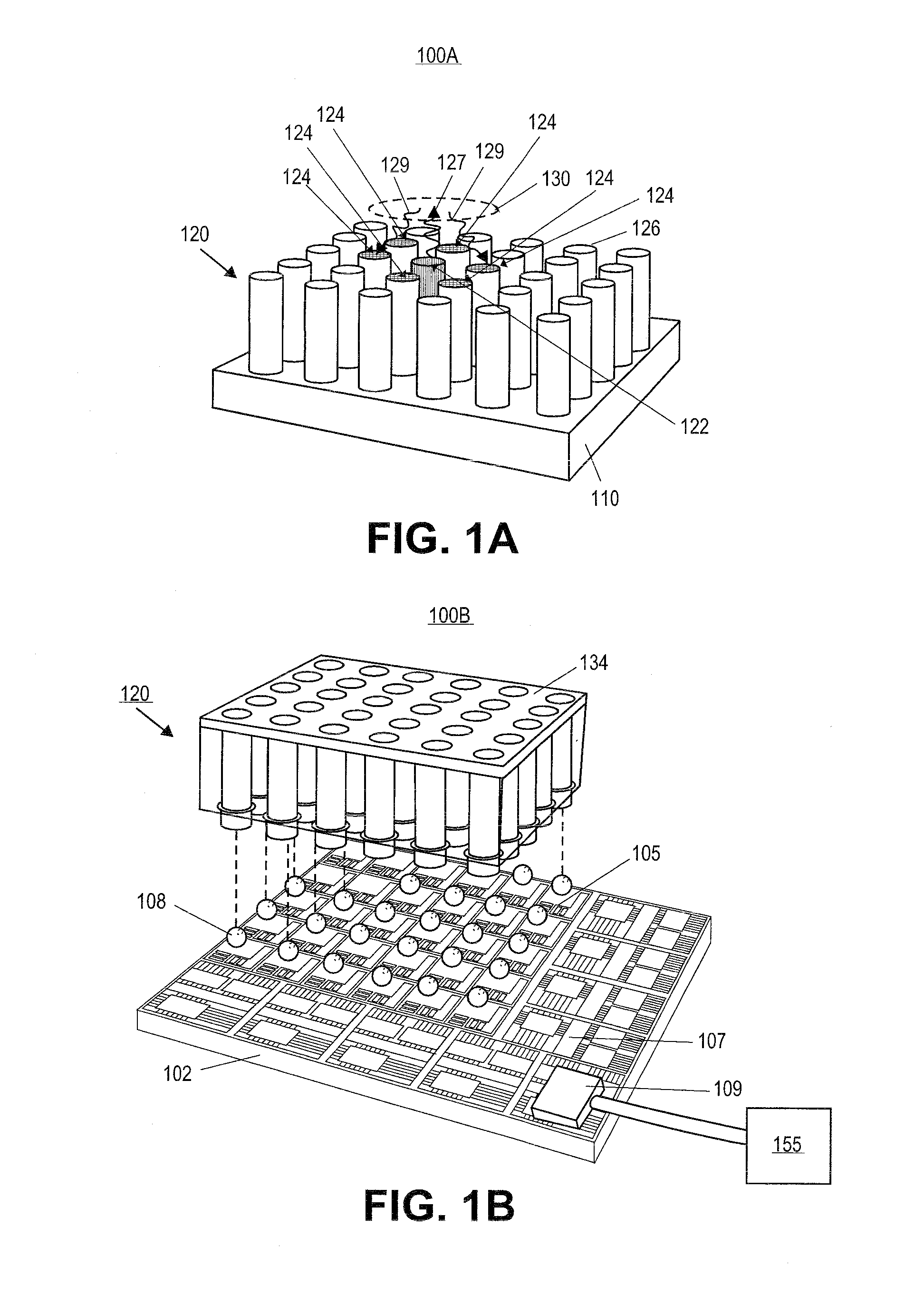
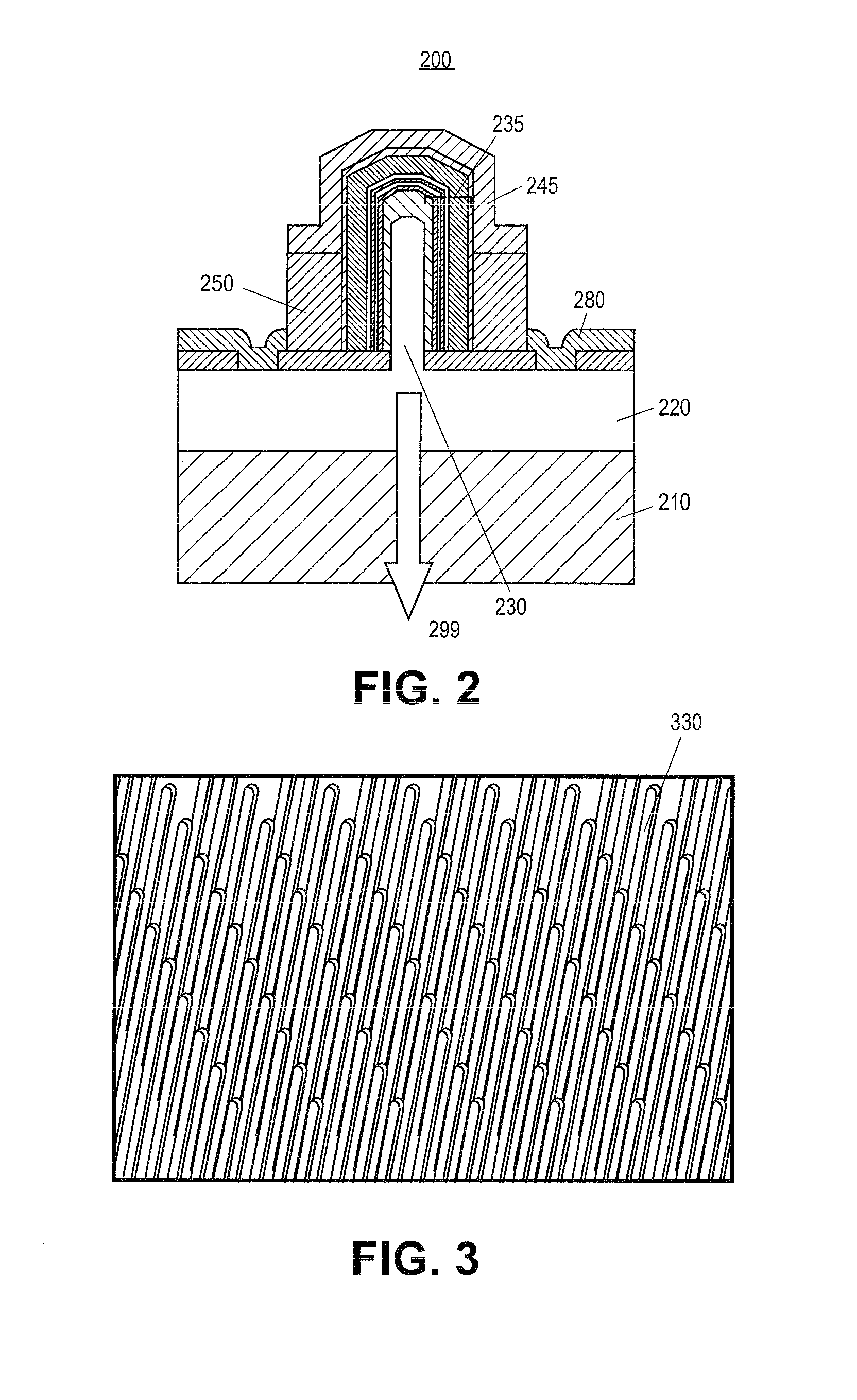
The present patent teaches a microscope device that includes a readout integrated circuit (ROIC) and a light emitting diode (LED) structure with a plurality of LED core-shell structures. Each LED core-shell structure includes a layered shell enveloping a nanowire core, which includes a multi-quantum-well (MQW) active region. The LED structure also includes a p-side electrode and a growth mask dielectric. The method of forming the LED structure includes forming a plurality of LED core-shell structures, with a doped buffer layer, a growth mask dielectric, a nanowire core, and a layered shell enveloping the nanowire core and including a MQW active region. The LED array can then be attached to the ROIC. The patent also describes a method for producing a magnified image of an object by simultaneously viewing it from two microscope devices. The microscope device includes an LED array and a second microscope device can be provided to allow simultaneous viewing of the object. The method includes steps to illuminate the object, collect reflected and transmitted light, and form image pixels. The technical effects of the patent include improved image quality and a more complete understanding of the structure and function of the microscope device.

Problems solved by technology

Such conventional optical microscopes, however, may have drawbacks and disadvantages for specific microscopic applications.
For example, when conventional optical microscopes are used to observe biological samples, the strong illumination power of the conventional optical microscopes may irreversibly degrade biological samples, e.g., living cells.
This is known as photo-toxicity in the prior art.

Method used


Image

  • Lens-less digital microscope
  • Lens-less digital microscope
  • Lens-less digital microscope

Examples


Embodiment Construction

[0004]1. Field of the Invention

[0005]This invention relates generally to solid-state microscope devices and, more particularly, relates to lens-less semiconductor-based digital microscope devices, systems, and methods for fabricating and using them.

[0006]2. Background of the Invention

[0007]A conventional optical microscope uses optical lenses to gather light from an illuminated object and provide a magnified image of that object to the viewer. An additional light source, that itself may require conditioning optics, is often used to illuminate the sample for the conventional optical microscopes.

[0008]Such conventional optical microscopes, however, may have drawbacks and disadvantages for specific microscopic applications. For example, when conventional optical microscopes are used to observe biological samples, the strong illumination power of the conventional optical microscopes may irreversibly degrade biological samples, e.g., living cells. This is known as photo-toxicity in the p...


PUM


Abstract

Exemplary embodiments provide microscope devices and methods for forming and using the microscope devices. The microscope device can include a light emitter array with each light emitter individually addressable to either emit or detect light signals. Magnified images of a sample object can be generated by a reflection mechanism and / or a transmission mechanism using one or more microscope devices in an imaging system. Real-time computer control of which microscope pixels are viewed can allow the user to digitally replicate the “fovea” function of human vision. Viewing an object from both sides in the double-sided microscope system and from multiple pixel positions can allow the microscope to reconstruct pseudo-3D images of the object.

Description

RELATED APPLICATIONS[0001]This application is a continuation-in-part of U.S. patent application Ser. No. 12 / 103,920, now copending, entitled “Solid State Microscope,” filed Apr. 16, 2008, which claims priority to U.S. Provisional Patent Applications Set. No. 60 / 913,927, filed Apr. 25, 2007, and Ser. No. 60 / 973,465, filed Sep. 19, 2007, all of which are hereby incorporated by reference in their entirety.[0002]This application also claims priority from U.S. Provisional Patent Application Ser. No. 61 / 276,400 filed Sep. 11, 2009, which is hereby incorporated by reference in its entirety.GOVERNMENT RIGHTS[0003]This invention was made with government support under Contract No. EEC0812056 awarded by the National Science Foundation (NSF), and under Contract No. HR0011-05-1-0006 awarded by the Defense Advanced Research Projects Agency (DARPA). The Government has certain rights in the invention.DESCRIPTION OF THE INVENTION[0004]1. Field of the Invention[0005]This invention relates generally t...

Claims


Application Information

Patent Timeline
IPC IPC(8): H04N7/18H04N9/47H04N5/243
CPCB82Y20/00G02B21/00H01L27/156B82Y15/00G02B21/0004G02B21/002G01Q60/22H01L33/24H01L33/18B82Y35/00
Inventor HERSEE, STEPHEN D.HAYAT, MAJEED M.SEN, PRADEEP
Owner STC UNM
Learn More