


Quick Research
Generate reliable direction feasibility study reports for your R&D in just a few steps.

Technical Q&A
Discover and master advanced knowledge NOW. Basics, ideas, possibilities, all at once.

Find Solutions
As an expert in R&D theories, this can generate solutions to your technical problems instantly.

Evaluate Feasibility
Analyze your overall solution with one click, know your potential R&D risks in advance.

Monitor Landscape
Get weekly tech updates, stay abreast of the latest tech innovations and key insights.
Memory controller, semiconductor storage device, and memory system including the memory controller and the semiconductor storage device for outputting temperature value in low power consumption mode
a technology of memory controller and temperature value, which is applied in the direction of digital storage, climate sustainability, instruments, etc., can solve the problems of reducing the effect of power consumption reduction by power down mode, requiring a lot of time to adjust (search) the correction value, and requiring a lot of time to detect optimal correction values, etc., to achieve the effect of reducing power consumption and delay amoun
- Summary
- Abstract
- Description
- Claims
- Application Information
AI Technical Summary
Benefits of technology
Problems solved by technology
Method used
Image

Examples
first exemplary embodiment
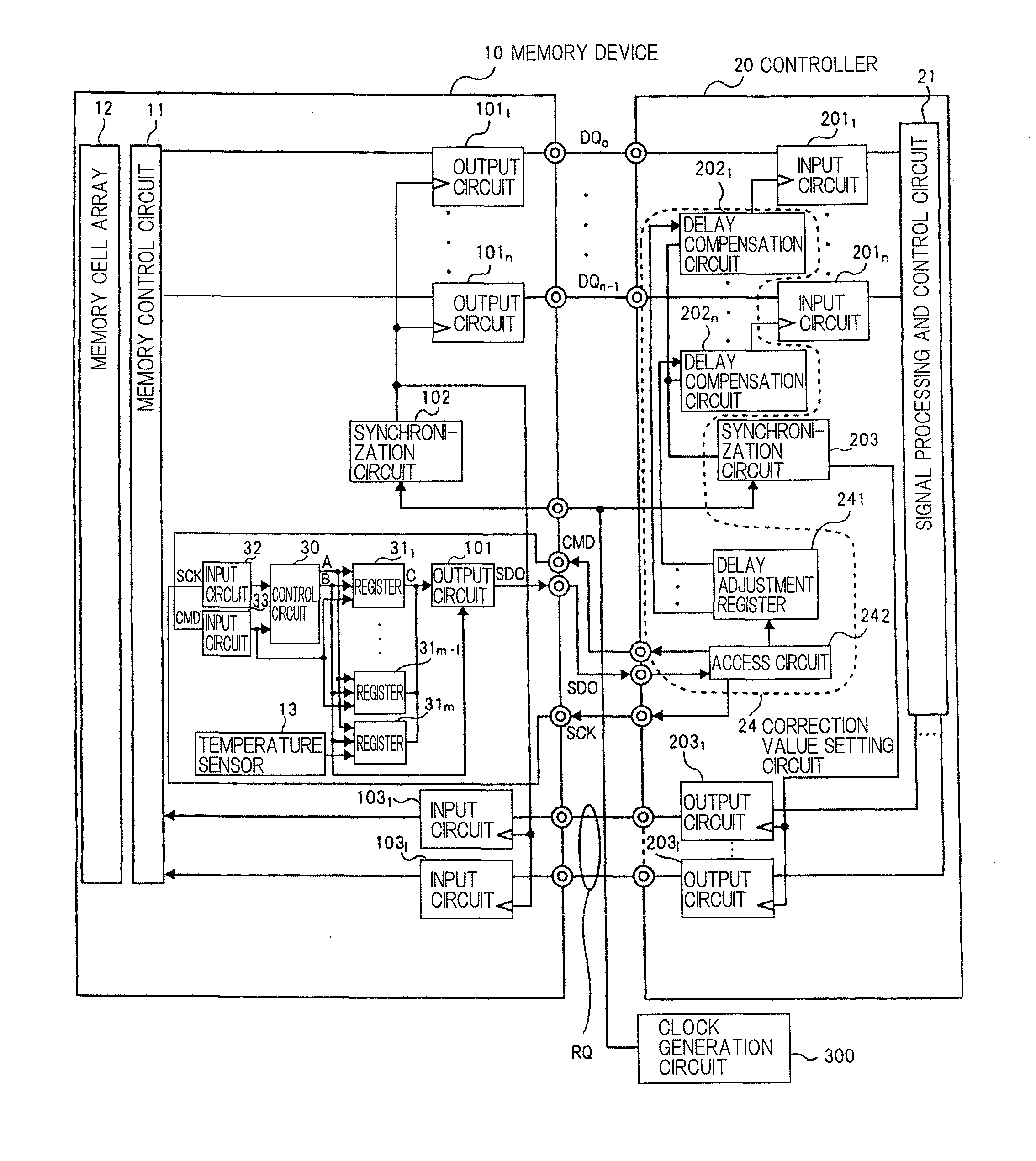
[0044]FIG. 2 is a block diagram showing a memory system as a first exemplary embodiment.
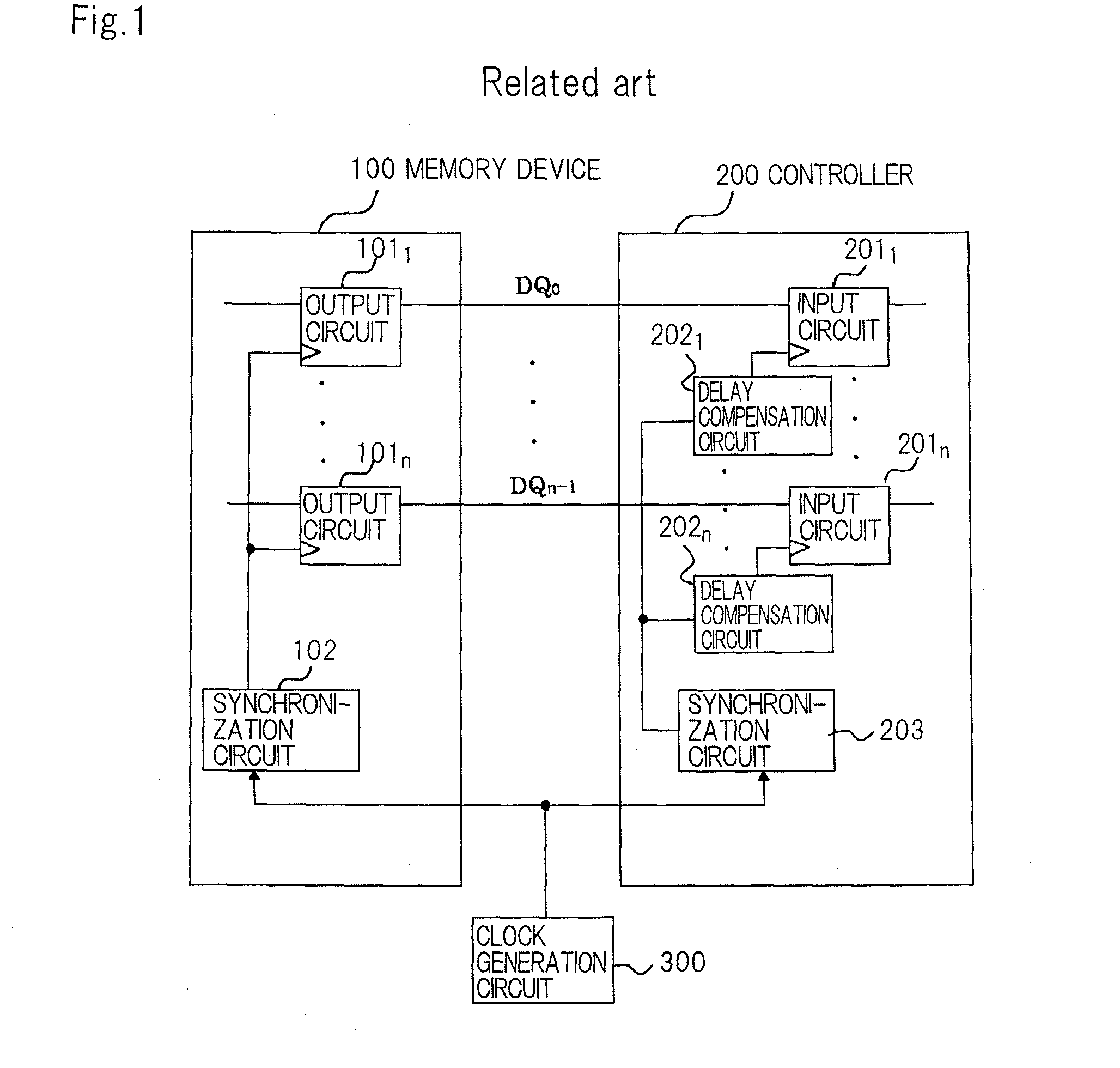
[0045]The memory system according to the first exemplary embodiment comprises memory device 10 as a semiconductor storage device, controller 20, and clock generation circuit 300.
[0046]Memory device 10 is a semiconductor storage device in which temperature sensor 13 is further installed in conventional memory device 100 shown in FIG. 1. In controller 20, correction value setting means 24 is further installed in conventional controller 200 shown in FIG. 1. In FIG. 2, the same configurations as the configurations shown in FIG. 1 are designated with the same reference numerals.
[0047]Temperature sensor 13 arranged in memory device 10 detects the temperature (internal temperature) of memory device 10, and correction value setting means 24 receives an output value (temperature of memory device 10) based on the detected temperature. Correction value setting means 24 sets correction values to delay compen...
second exemplary embodiment
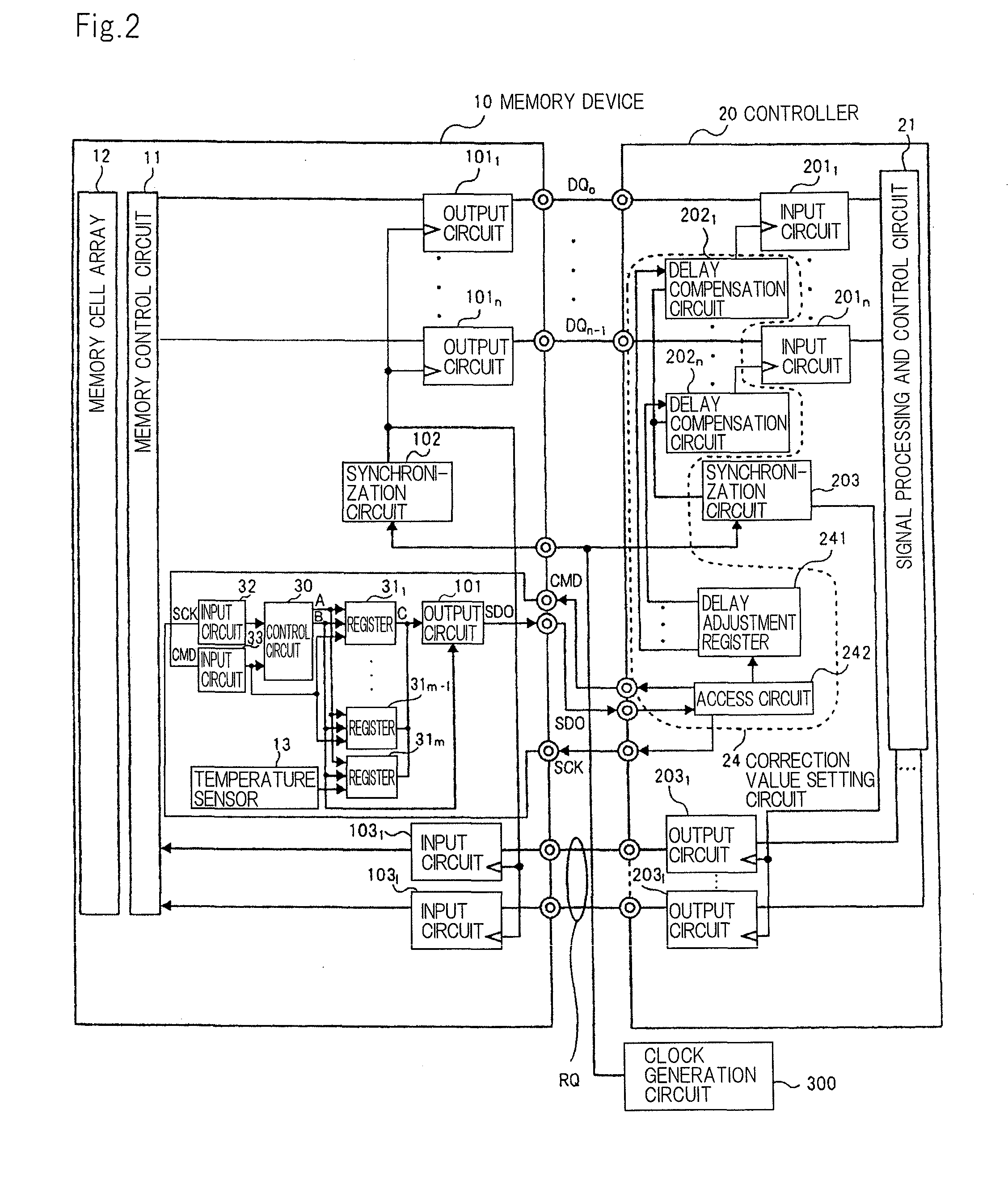
[0076]FIG. 5 is a block diagram showing a configuration of a memory system as a second exemplary embodiment.
[0077]In the memory system of the exemplary embodiment, mode setting means 25 is further installed in the configuration of the first exemplary embodiment, and part of the adjustment operation of the correction values is different from that in the first exemplary embodiment.
[0078]Mode setting means 25 is configured to set the operation mode of memory device 10. The normal operation mode and the power down mode can be set as the operation mode by mode setting means 25. Writing operations of data to memory device 10 and reading operations of data from memory device 10 (output operations of data by output circuits 1011 to 101n) are performed in the normal operation mode. The input and output operations of data of memory device 10 are not performed in the power down mode. Command signal CMD, etc. shown in FIG. 2 are used to set the mode.
[0079]If a change in the mode is requested ba...
third exemplary embodiment
[0083]Although the configuration of a memory system as a third exemplary embodiment is the same as that of the second exemplary embodiment, part of the adjustment operation of the correction values is different.
[0084]Mode setting means 25 supplies a set mode signal to access circuit 242 once the mode is set and supplies an initialization signal indicative of the initialization to access circuit 242 upon initialization.
[0085]Access circuit 242 determines whether the period is the power down mode setting period based on the set mode signal and supplies the mode period determination result to delay adjustment register 241. When the initialization signal is received, access circuit 242 acquires the temperature value of memory device 10 from temperature sensor 13.
[0086]The output of output circuits 1011 to 101n and the output of compensation circuits 2021 to 202n are also supplied to delay adjustment register 241.
[0087]When the initialization signal (resent signal) is received from acces...
PUM
 Abstract
Description
Claims
Application Information
 - R&D Engineer
- R&D Manager
- IP Professional
- Industry Leading Data Capabilities
- Powerful AI technology
- Patent DNA Extraction
Browse by: Latest US Patents, China's latest patents, Technical Efficacy Thesaurus, Application Domain, Technology Topic, Popular Technical Reports.
© 2024 PatSnap. All rights reserved.Legal|Privacy policy|Modern Slavery Act Transparency Statement|Sitemap|About US| Contact US: help@patsnap.com