
Method for manufacturing vertical-channel tunneling transistor

a manufacturing method and technology of transistor, applied in semiconductor devices, diodes, electrical devices, etc., can solve the problems of mos transistor channel length also reducing continuously, semiconductor chip performance decline, and inability to work, so as to improve device channel length control.

Active Publication Date: 2013-11-19
FUDAN UNIV
View PDF14 Cites 1 Cited by
  • Summary
  • Abstract
  • Description
  • Claims
  • Application Information

AI Technical Summary

Benefits of technology

The present invention provides a method for making a vertical-channel tunneling transistor that can better control the device channel length. This method is simple, easy to control, and can reduce production costs.

Problems solved by technology

However, with the increase of the integration degree of semiconductor chips, the channel length of MOS transistor is also reducing continuously, and the semiconductor chip performances will decline, or even be unable to work due to the short channel effect when the channel length of the MOS transistor becomes extremely short.
Since the depth of the junction implanted is difficult to control, the channel length is also difficult to control.

Method used


Image

  • Method for manufacturing vertical-channel tunneling transistor
  • Method for manufacturing vertical-channel tunneling transistor
  • Method for manufacturing vertical-channel tunneling transistor

Examples


Embodiment Construction

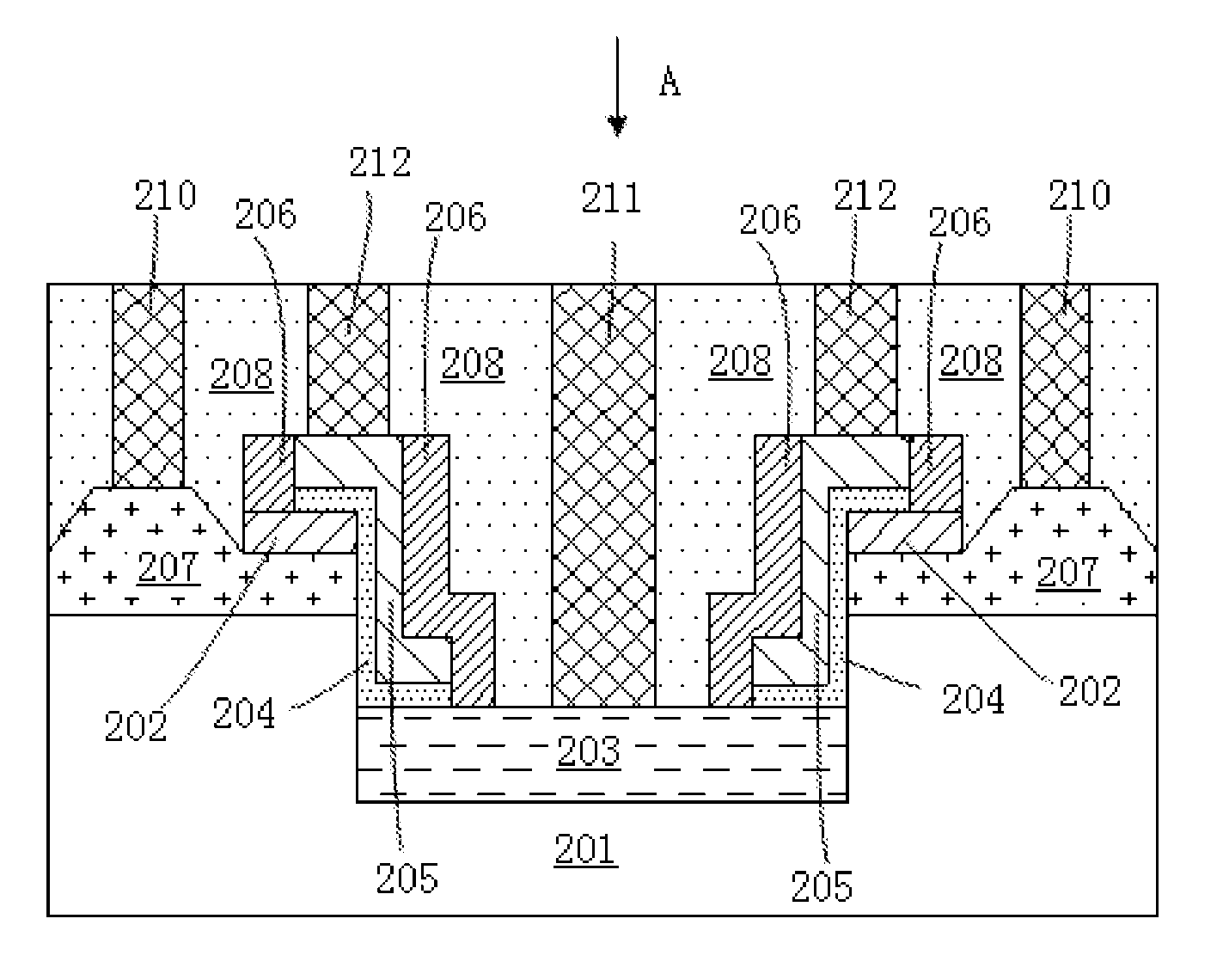
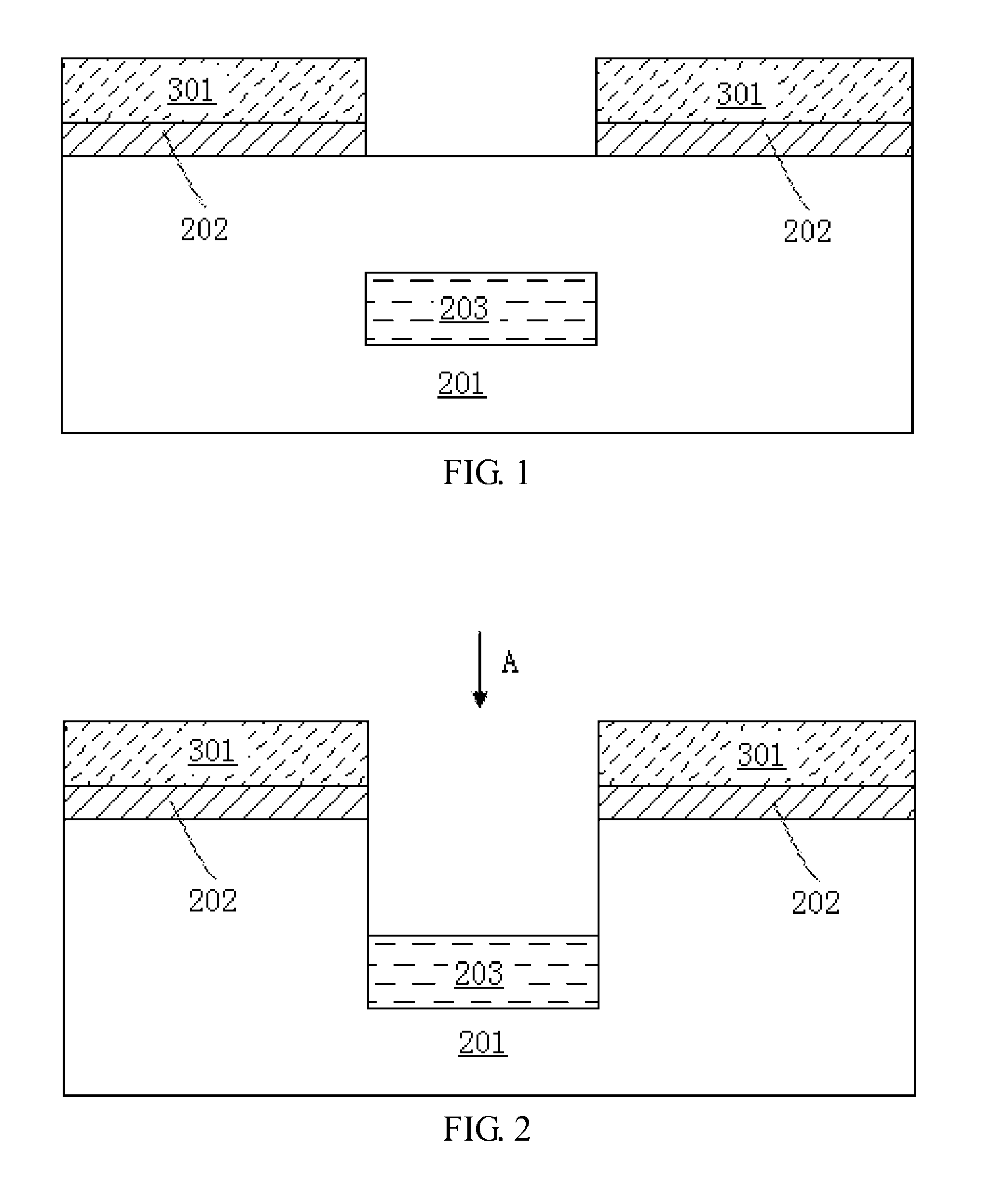
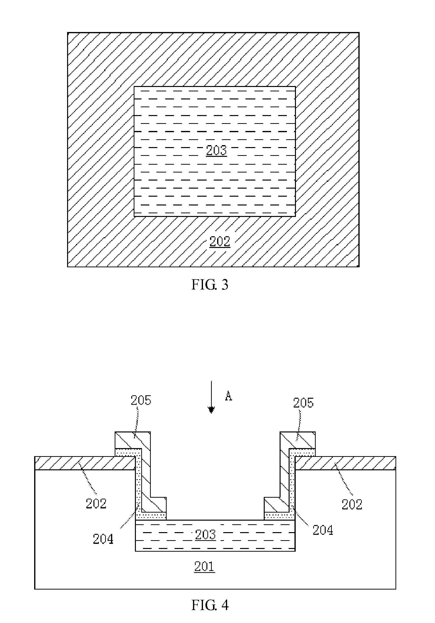
[0032]An exemplary embodiment of the present invention is further detailed herein by referring to the drawings. In the drawings, the thicknesses of the layers and regions are either zoomed in for the convenience of description, so they shall not be considered as the true size. Although these drawings cannot accurately reflect the true size, they still reflect the relative positions among the regions and components completely, especially the up-down and adjacent relations.

[0033]The reference diagrams are the schematic diagrams of the idealized embodiments of the present invention, so the embodiments shown in the present invention shall not be limited to specific shapes in areas shown in the drawings, while they shall include the obtained shapes such as the deviation caused by manufacturing. For instance, curves obtained through etching are often bent or rounded, while in the embodiments of the present invention, they are all presented in rectangles, and what the drawings present is s...


PUM


Abstract

The present invention belongs to the technical field of semiconductors and specifically relates to a method for manufacturing a vertical-channel tunneling transistor. In the present invention, the surrounding gate gate structure improves the control capacity of the gate and the source of narrow band gap material can enhance the device driving current. The method for manufacturing a vertical-channel tunneling transistor put forward by the present invention capable of controlling the channel length precisely features simple process, easy control and reduction of production cost.

Description

[0001]This application claims benefit of Serial No. 201110410898.6, filed 12 Dec. 2011 in China and which application is incorporated herein by reference. To the extent appropriate, a claim of priority is made to the above disclosed application.BACKGROUND OF THE INVENTION[0002]1. Technical Field[0003]The present invention belongs to the technical field of semiconductor devices, relates to a method for manufacturing a tunneling field effect transistor, and more especially, to a method for manufacturing a vertical-channel tunneling transistor using narrow band gap materials as the source.[0004]2. Description of Related Art[0005]In recent years, microelectronic technology with silicon integrated circuits as their core has developed rapidly, the and the development of the integrated circuit chip basically follows the Moore's law, namely the integration degree of semiconductor chips increases at a speed of doubling every 18 months. However, with the increase of the integration degree of ...

Claims


Application Information

Patent Timeline
Patent Type & Authority Patents(United States)
IPC IPC(8): H01L21/336
CPCH01L29/66356H01L29/7391H01L29/165H01L29/0692
Inventor WANG, PENGFEILIN, XILIU, WEISUN, QINGQINGZHANG, WEI
Owner FUDAN UNIV
Learn More