
Nonvolatile memory unit, manufacturing method, and opertion method

A non-volatile, method-of-operation technology, applied in semiconductor/solid-state device manufacturing, electrical solid-state devices, semiconductor devices, etc., can solve problems such as inability to increase component integration and large size, achieve high electron injection efficiency and increase integration , Improve the effect of integration

Inactive Publication Date: 2007-02-21
POWERCHIP SEMICON CORP
View PDF0 Cites 5 Cited by
  • Summary
  • Abstract
  • Description
  • Claims
  • Application Information

AI Technical Summary

Problems solved by technology

[0006] However, since the split gate structure requires a larger split gate area and has a larger memory cell size, its memory cell size is larger than that of a memory cell with a stacked gate, which causes the problem of not being able to increase the integration of components.

Method used


Image

  • Nonvolatile memory unit, manufacturing method, and opertion method
  • Nonvolatile memory unit, manufacturing method, and opertion method
  • Nonvolatile memory unit, manufacturing method, and opertion method

Examples


Embodiment Construction

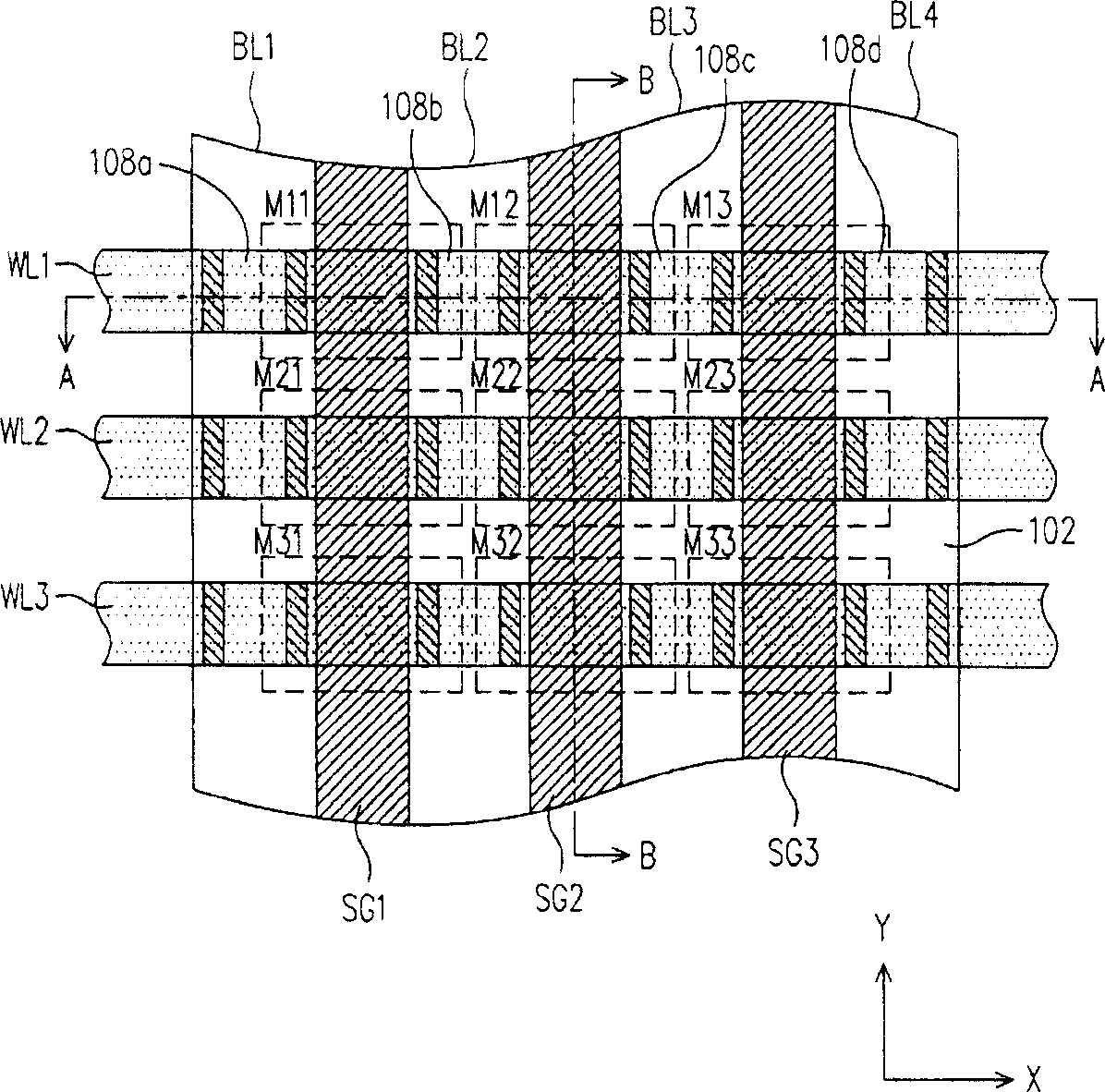
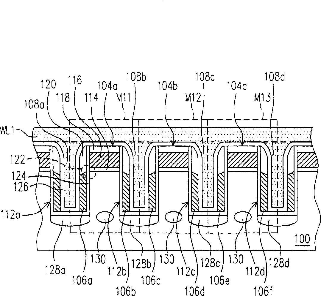
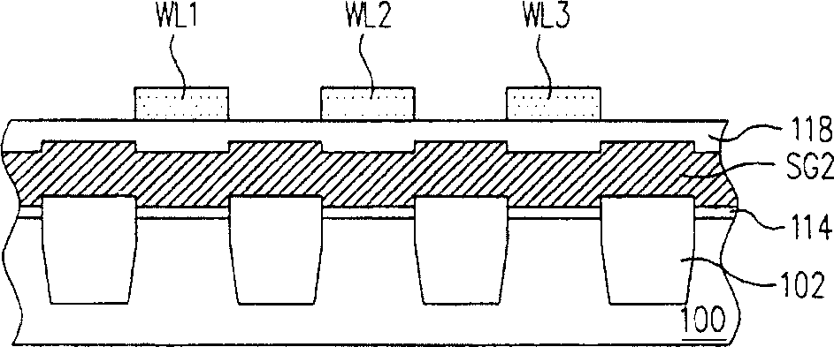
[0075] Figure 1A Shown is a top view of a preferred embodiment of the non-volatile memory of the present invention. Figure 1B for depicted as Figure 1A Structural cross-section along line A-A'. Figure 1C for depicted as Figure 1A The structural cross-section along the line B-B' in the middle.

[0076] Please refer to Figure 1A , the non-volatile memory array of the present invention includes a substrate 100, a plurality of memory cells M11-M33, a plurality of word lines WL1-WL3, a plurality of select gate lines SG1-SG3, and bit lines BL1-BL4.

[0077] The substrate 100 is, for example, a silicon substrate, and a plurality of device isolation structures 102 are disposed in the substrate 100 to define active regions. These component isolation structures 102 are arranged in parallel and extend towards the X direction

[0078] The memory cells M11-M33 are disposed on the substrate 100 and arranged in a row / column array. The multiple word lines WL1 - WL3 are respectively c...


PUM


Abstract

The non-volatile memory includes substrate, selection grid electrode, two charge storage layers, two regions of source electrode / drain electrode and control grid electrodes. At least two grooves are setup in the substrate. The selection grid electrode is setup on substrate between the two grooves. Two charge storage layers are setup at sidewalls of the selection grid electrodes adjacent to two grooves respectively. Two regions of source electrode / drain electrode are setup on substrate of base of two grooves. Being setup on substrate, selection grid electrode is filled to two grooves.

Description

technical field [0001] The invention relates to a semiconductor element, in particular to a non-volatile memory and its manufacturing method and operation method. Background technique [0002] Among all kinds of non-volatile memory products, it has the advantages of multiple data storage, reading, erasing, etc., and the stored data will not disappear after power off. Program read-only memory (EEPROM) has become a memory element widely used in personal computers and electronic equipment. [0003] A typical EEPROM uses doped polysilicon to make a floating gate (Floating Gate) and a control gate (Control Gate). Moreover, the floating gate is separated from the control gate by a dielectric layer, and the floating gate is separated from the substrate by a tunneling oxide layer. When writing / erasing (Write / Erase) data to the flash memory, by applying a bias voltage to the control gate and the source / drain region, electrons are injected into the floating gate or electrons are rel...

Claims


Application Information

Patent Timeline
Patent Type & Authority Applications(China)
IPC IPC(8): H01L21/8238H01L21/8247H01L21/336H01L27/105H01L27/115H01L29/78H10B69/00
Inventor 王炳尧赖亮全
Owner POWERCHIP SEMICON CORP
Learn More