
Inspection method and apparatus, lithographic apparatus, lithographic processing cell and device manufacturing method

a technology of lithographic apparatus and manufacturing method, which is applied in the direction of instruments, printers, and spectrum investigation. it can solve the problems of lithographic apparatus, lithographic apparatus errors that cannot be easily detected or quantified from resist patterns, and problems for the resulting produ

Active Publication Date: 2013-10-08
ASML NETHERLANDS BV
View PDF23 Cites 34 Cited by
  • Summary
  • Abstract
  • Description
  • Claims
  • Application Information

AI Technical Summary

Benefits of technology

The patent text describes a need for an effective system and method to provide a radiation source that can be used with smaller targets to measure overlay without losing diffraction spectra information. This would help in ensuring accurate and reliable measurements during the manufacturing process.

Problems solved by technology

Second, the measurements may allow errors in the lithographic apparatus, e.g., illumination settings or exposure dose, to be detected and corrected for in subsequent exposures.
However, many errors in the lithographic apparatus may not easily be detected or quantified from the patterns printed in resist.
If there is an overlay, the overall structure after exposure of all the layers will not be formed accurately and may cause problems for the resulting product.
As it is the parts of the diffraction orders that do not overlap that give the information, the overlapping parts are not used for measurement and are therefore “wasted”.
However, even using an annular radiation beam may not prevent some of the beam from being lost because as targets get smaller, parts of the annular beam should be discarded if it contains information from neighboring targets or even any off-target surface.
The beam may not simply be shrunk to fit smaller target sizes, as information from higher diffraction orders is likely to be lost.

Method used


Image

  • Inspection method and apparatus, lithographic apparatus, lithographic processing cell and device manufacturing method
  • Inspection method and apparatus, lithographic apparatus, lithographic processing cell and device manufacturing method
  • Inspection method and apparatus, lithographic apparatus, lithographic processing cell and device manufacturing method

Examples


Embodiment Construction

[0038]This specification discloses one or more embodiments that incorporate the features of this invention. The disclosed embodiment(s) merely exemplify the invention. The scope of the invention is not limited to the disclosed embodiment(s). The invention is defined by the claims appended hereto.

[0039]The embodiment(s) described, and references in the specification to “one embodiment,”“an embodiment,”“an example embodiment,” etc., indicate that the embodiment(s) described may include a particular feature, structure, or characteristic, but every embodiment may not necessarily include the particular feature, structure, or characteristic. Moreover, such phrases are not necessarily referring to the same embodiment. Further, when a particular feature, structure, or characteristic is described in connection with an embodiment, it is understood that it is within the knowledge of one skilled in the art to affect such feature, structure, or characteristic in connection with other embodiments...

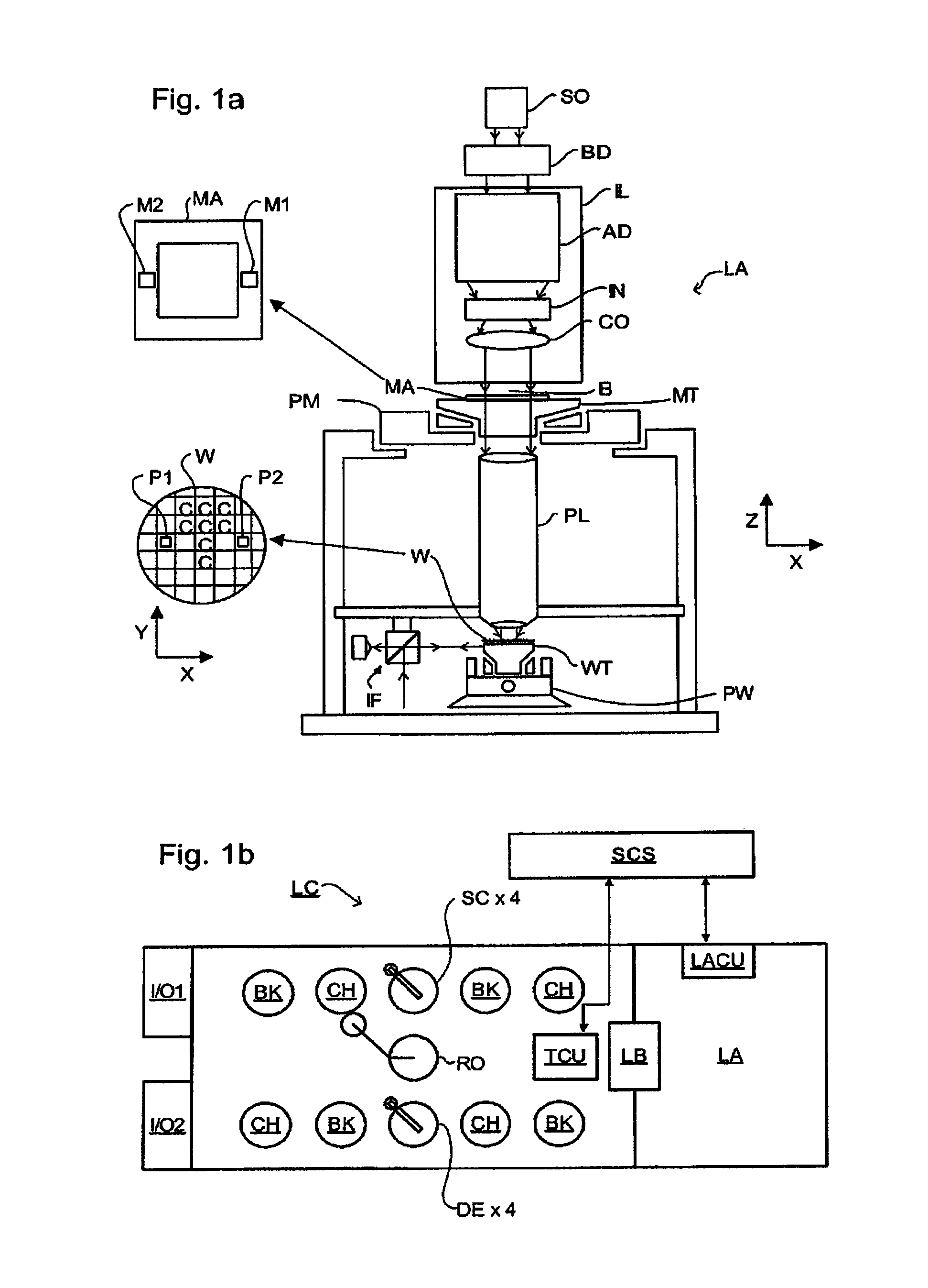
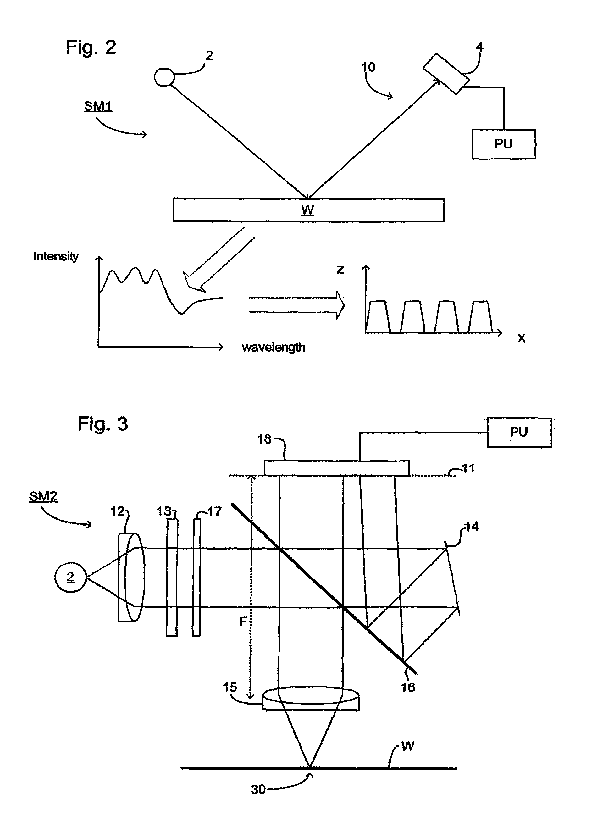

PUM


Abstract

An apparatus and method to determine a property of a substrate by measuring, in the pupil plane of a high numerical aperture lens, an angle-resolved spectrum as a result of radiation being reflected off the substrate. The property may be angle and wavelength dependent. The radiation that is reflected off the substrate is radially polarized.

Description

CROSS REFERENCE TO RELATED APPLICATIONS[0001]This is a Continuation of U.S. application Ser. No. 12 / 259,536, filed Oct. 28, 2008 (now abandoned), which claims benefit of under 35 U.S.C. §119(e) to U.S. Provisional Patent Application No. 60 / 996,356, filed Nov. 13, 2007, which are incorporated by reference herein in their entirety.BACKGROUND[0002]1. Field of the Invention[0003]The present invention relates to methods of inspection usable, for example, in the manufacture of devices by lithographic techniques and to methods of manufacturing devices using lithographic techniques.[0004]2. Related Art[0005]A lithographic apparatus is a machine that applies a desired pattern onto a substrate, usually onto a target portion of the substrate. A lithographic apparatus can be used, for example, in the manufacture of integrated circuits (ICs). In that instance, a patterning device, which is alternatively referred to as a mask or a reticle, may be used to generate a circuit pattern to be formed on...

Claims


Application Information

Patent Timeline
Patent Type & Authority Patents(United States)
IPC IPC(8): G01J4/00
CPCG01N21/47G01N21/95G01N21/956G03F7/70625G03F7/70633G01N21/21
Inventor JORDANOSKA, CVETANKA
Owner ASML NETHERLANDS BV
Learn More