Functionally graded biocompatible coating and coated implant
a biocompatible coating and implant technology, applied in the field of biocompatible coatings, can solve the problems of loosened implant, loss of implanted teeth, infection around the implant,
- Summary
- Abstract
- Description
- Claims
- Application Information
AI Technical Summary
Benefits of technology
Problems solved by technology
Method used
Image
Examples
example 1
Preparation of Coated Substrate
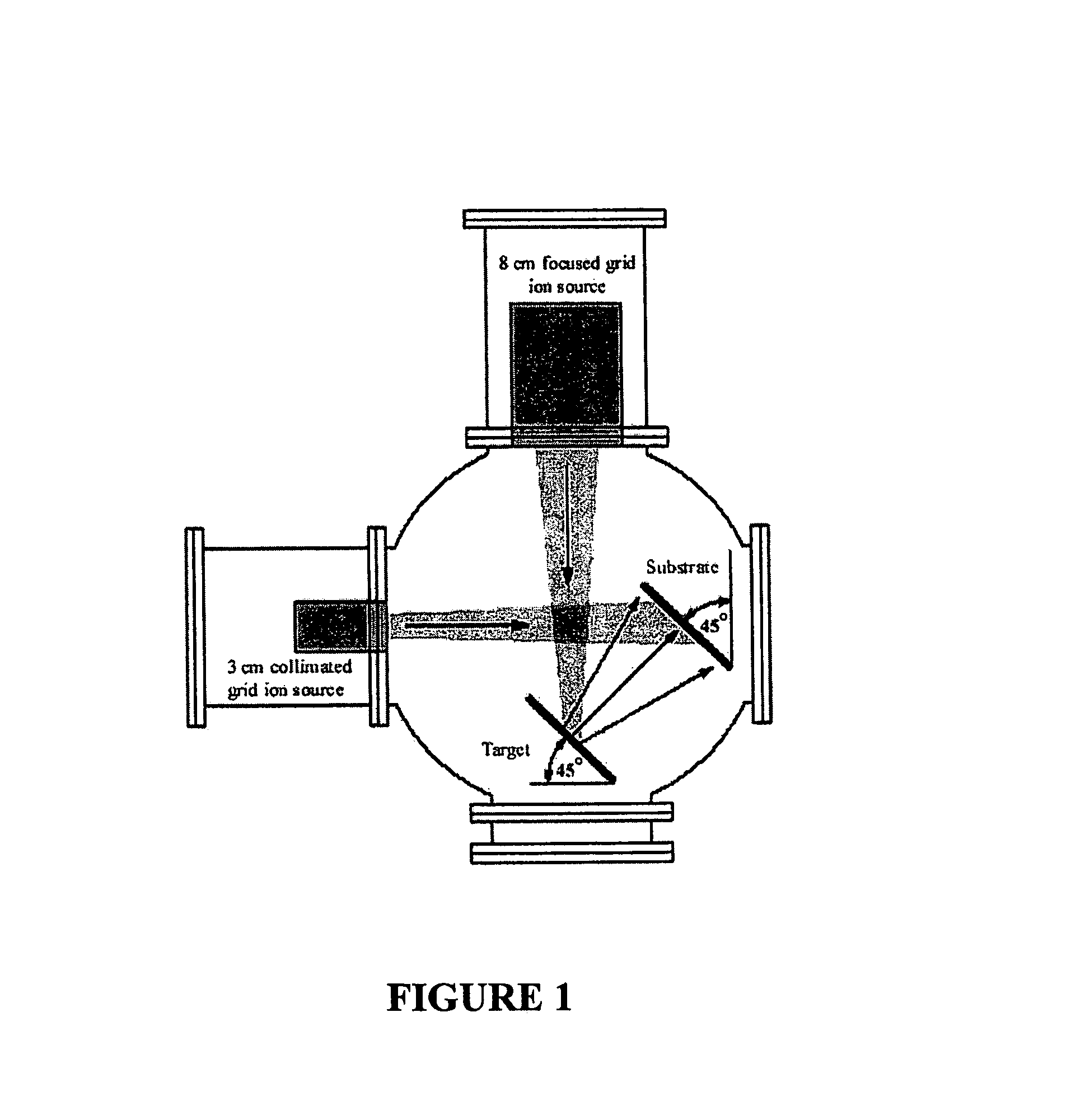
[0108]A coated substrate was prepared by depositing a hydroxyapatite film on a silicon substrate in a dual ion beam sputtering system as shown in FIG. 1. The base pressure of the dual ion beam sputtering system was set at 9×10⁻⁷ Torr. A 15.24 cm diameter hydroxyapatite target recessed into a stainless steel holder was used as the hydroxyapatite source.
[0109]For the duration of the deposition process, the primary ion source was set at 1000V, and a gas flow of 3 sccm was provided to each ion source bringing the background pressure of the system to approximately 4×10⁻⁴ Torr. The assist beam was initially set to 1000V. After 10 minutes of deposition, the assist beam was set to 400V, and it remained at that setting for the remainder of the deposition.
[0110]For the first 2 hours of deposition, the substrate heater was set at 700° C. After two hours of deposition, the substrate heater was reduced to 500° C. After an additional 2 hours, the heater was complete...
example 2
Structural Analysis of Hydroxyapatite Film on Coated Substrate
[0112]The cross-sectional structure of the HA film prepared in Example 1 is shown in FIG. 2. The figure provides a TEM cross-sectional image of the functionally graded HA film. The film has an overall thickness of 875 nm, and on visual inspection, the film can be seen to include a number of distinct layers. The silicon substrate is covered by a thin amorphous layer of silicon dioxide (about 12 nm thick), followed by a coarse crystalline HA layer (210 nm thick). On top of that is a fine crystalline HA layer (140 nm thick), followed by a layer of amorphous HA mixed with very fine nano-structure HA grains (513 nm thick).
[0113]As can be seen in FIG. 2, the degree of crystallinity decreases from the bottom layer (in contact with the substrate) to the top layer. The bottom layer comprises predominantly crystalline HA, while the top layer comprises predominantly amorphous HA. Further, the crystal grain size also decreases from t...
example 3
Preparation of Comparative Coated Substrate
[0116]For use as a comparative to the coating of the invention, a calcium phosphate film was sputtered on a cleaned glass surface using a CMS-18 radiofrequency magnetron sputtering system. The target used in the sputtering process was a 101.6 mm diameter sintered HA target on a copper backing. The base pressure in the sputtering chamber was about 6.5×10⁻⁶ Torr. Sputter-deposition was performed using a process pressure of about 1.0 to about 1.5 mbar and a sputtering power of 200 W for 7 hours. A coating rate of 60 nm per hour was observed. After sputtering, the coated samples were subjected to post-deposition heat treatment at 500° C. for 30 minutes using a Thermolyne 48000 furnace to prepare a crystalline phase coating. The post-deposition heat treatment resulted in a crystallinity of 62% (±2%), which was confirmed by X-ray diffraction.
PUM
| Property | Measurement | Unit |
|---|---|---|
| diameter | aaaaa | aaaaa |
| thickness | aaaaa | aaaaa |
| thickness | aaaaa | aaaaa |
Abstract
Description
Claims
Application Information
 - R&D
- Intellectual Property
- Life Sciences
- Materials
- Tech Scout
- Unparalleled Data Quality
- Higher Quality Content
- 60% Fewer Hallucinations
Browse by: Latest US Patents, China's latest patents, Technical Efficacy Thesaurus, Application Domain, Technology Topic, Popular Technical Reports.
© 2025 PatSnap. All rights reserved.Legal|Privacy policy|Modern Slavery Act Transparency Statement|Sitemap|About US| Contact US: help@patsnap.com


