Detection circuit and manufacturing method for LCD panel

a detection circuit and manufacturing method technology, applied in the direction of spark plugs, lighting and heating apparatus, instruments, etc., can solve the problems of increasing difficult to dispose of so many test lines and testing signal pads, etc., to achieve sufficient current supply capacity, simplify the detection circuit, and increase the capacity of each of the pads

Active Publication Date: 2013-09-10
TCL CHINA STAR OPTOELECTRONICS TECH CO LTD
View PDF10 Cites 6 Cited by
  • Summary
  • Abstract
  • Description
  • Claims
  • Application Information

AI Technical Summary

Benefits of technology

[0036]The beneficial effects of the present invention are: The inventors of the present application proposed earlier to connect the same test lines or the PSVA lines of the different panel units 21 in parallel to a same circuit line. Each of the same circuit lines connects to one pad. The simplified detection circuit makes each of the pads connect to the N×m test lines or PSVA lines such that the capacitive load of each of the pad is increased. Therefore, the external power supply must have sufficient current supply capacity to avoid the problem of insufficient driving current. Furthermore, in the process of the testing, the N panel units 21 are simultaneously applying, the testing so that when one of the N panel units 21 has a short circuit situation, it is unable to distinguish the panel unit having the short circuit situation. The inventors of present application base on the above situation. In the present invention, the testing pad collection and the switch collection are disposed in the detection circuit so that the signal line of each of the panel units connects to the corresponding testing signal pad of the testing, pad collection respectively through the input terminal and the output terminal of the control switch of the switch collection, and the control terminal of the control switch electrically connects to the control signal pad. It can selectively apply a distinguishable testing to one or a plurality of the panel units, simplifying the detection circuit, reducing the load of the detection circuit at the same time. However, it can also clearly distinguish the panel unit having short circuit.

Problems solved by technology

However, when the large combined glass 10 has more panel units 11 (i.e., the larger number of N) or the utilization rate of the large combined glass 10 is higher, the number oldie test lines or testing, signal pads will increase, it will be difficult to dispose so many test lines and testing signal pads on the large combined glass 10 at this time.

Method used


Image

  • Detection circuit and manufacturing method for LCD panel
  • Detection circuit and manufacturing method for LCD panel
  • Detection circuit and manufacturing method for LCD panel

Examples


Embodiment Construction

[0043]A detection circuit in the assembly process of an LCD panel of the present invention can simplify the detection circuit, and reduce the load of the detection circuit, and also can clearly distinguish the panel unit having short circuit.

[0044]The following combines drawings and embodiments for detail description of the present invention.

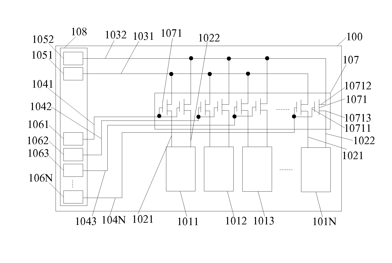
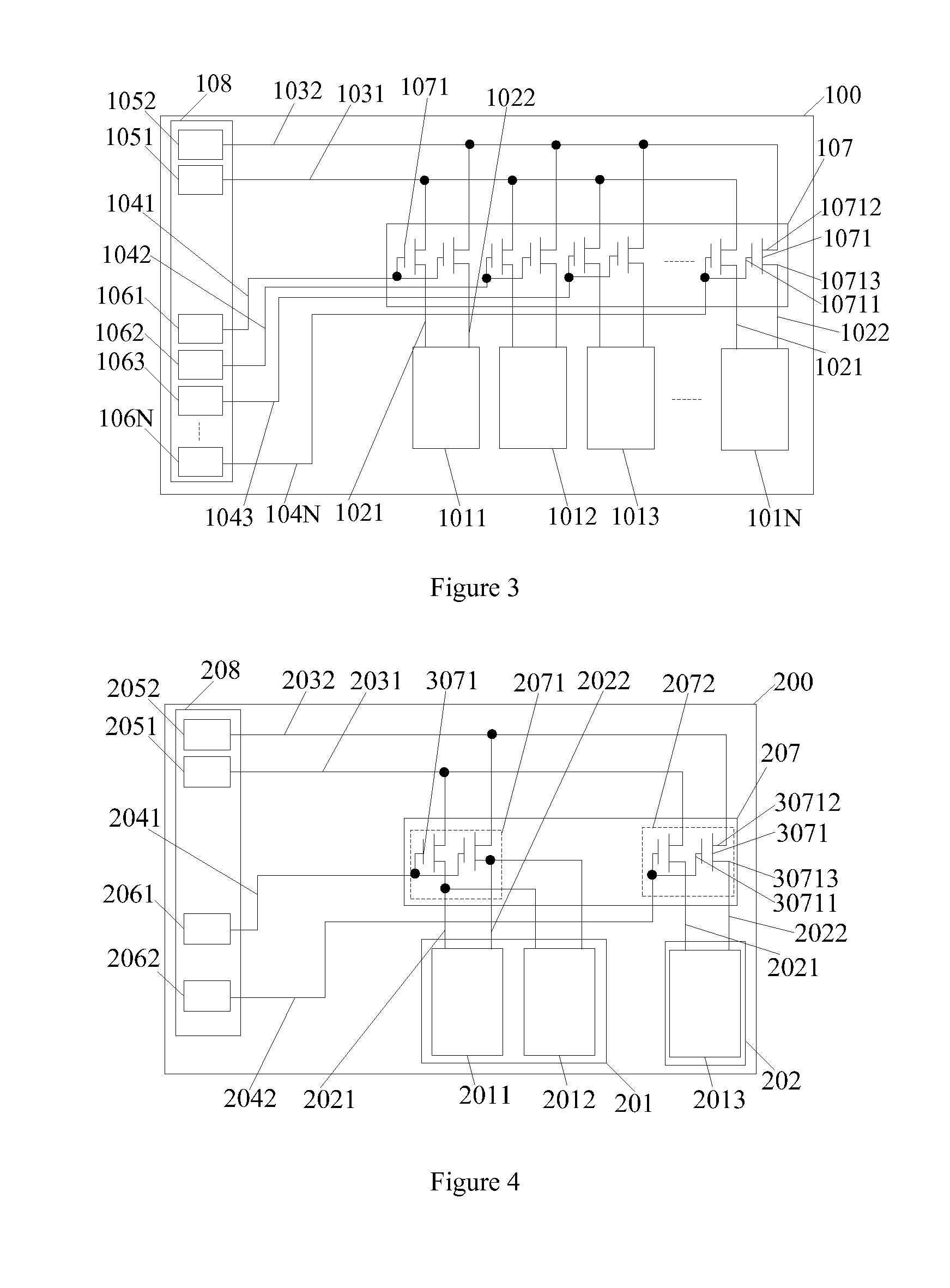
[0045]With reference to FIG. 3, in one embodiment of the detection circuit of the assembly process of the present invention, the detection circuit is used to apply a testing to the combined substrate 100 having multiple panel units. The testing includes an array testing or a PSVA testing for the multiple panel units.

[0046]Specifically, the combined substrate 100 including:

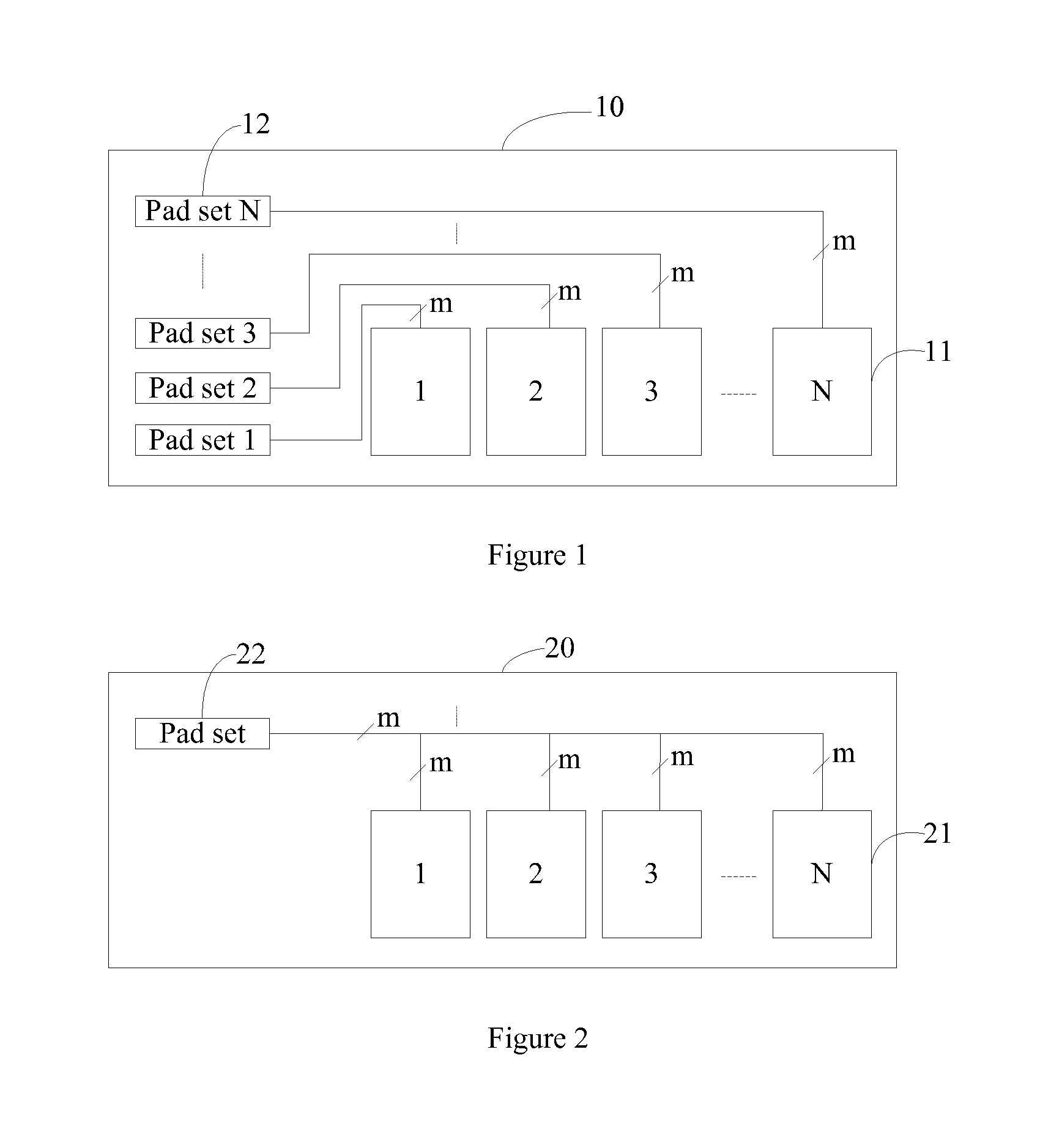
[0047]N (N is greater than or equal to 2) panel units, respectively, a panel unit 1011 to a panel unit 101N. Wherein, a panel unit 101k (k less than or equal to N for representing the k-th panel unit of the N panel units) comprises at least one signal line. Using two signal lin...


PUM

PropertyMeasurementUnit
current supply capacityaaaaaaaaaa
electricallyaaaaaaaaaa
equivalent structuresaaaaaaaaaa

Abstract

The present invention discloses a detection circuit in the assembly process of an LCD panel. Through the testing pad collection and the switch collection, the signal line of each of the panel units connects to the corresponding testing signal pad of the testing pad collection respectively through the input terminal and the output terminal of the control switch of the switch collection, and the control terminal of the control switch electrically connects to the control signal pad in order to selectively apply an individual testing to one of the panel units. The present invention also provides a manufacturing method for an LCD panel. Accordingly, the present invention can simplify the detection circuit and reduce the load of the detection circuit.

Description

BACKGROUND OF THE INVENTION[0001]1. Field of the Invention[0002]The present invention relates to the field of liquid crystal display (LCD) technology, and more particularly to a detection circuit and a manufacturing method for an LCD panel.[0003]2. Description of Related Art[0004]The liquid crystal display manufacturing process is generally divided into an array process, an assembly process, and a module process. The array process is for manufacturing a glass substrate made of glass substrate and required for LCD device such that it combines a color filter substrate, and attachment after injecting liquid crystal between the two substrates in order to form a large combined glass. Then, the large combined glass is cut to form multiple LCD panels. In the module process, assembling the LCD panel formed after being cut with a hack frame and multiple parts to form an LCD device.[0005]In assembly process, after forming the large combined glass and before cutting the large combined glass, i...

Claims


Application Information

Patent Timeline
Patent Type & Authority Patents(United States)
IPC IPC(8): H01J9/42G02F1/13G09G3/36G01R31/00
CPCG09G3/006G09G3/36G02F2001/136254G02F1/136254
Inventor CHEN, CHENG-HUNG
Owner TCL CHINA STAR OPTOELECTRONICS TECH CO LTD
Why Eureka
Try Eureka