Communication device

a communication device and chip antenna technology, applied in the direction of antennas, antenna details, electrically short antennas, etc., can solve the problems of deteriorating the ability of the chip antenna to receive radio waves of a desired wavelength, difficult to have a sufficient distance between ground wirings, and inability to achieve sufficient effects, so as to reduce the noise degree, reduce the influence of noise on the chip antenna, and the effect of oscillation of the power amplifier

Inactive Publication Date: 2013-08-06
KYOCERA CORP
View PDF14 Cites 0 Cited by
  • Summary
  • Abstract
  • Description
  • Claims
  • Application Information

AI Technical Summary

Benefits of technology

[0025]According to the present invention, an oscillation of the power amplifier is avoided by attaching a radio wave absorption body to the conductive body, hence it is possible to solve the new problem, that is an oscillation of the power amplifier, without deteriorating a function of reducing the influence of noises on the chip antenna.
[0026]In addition, in accordance with the present invention, by providing the conductive body, it is possible to reduce the degree of the noise that is generated by the closely installed devices and comes into the antenna chip.
[0027]Hence, by applying a low cost and easy solution of attaching a conductive body to the existing constitution, it is possible to reduce the influence of the noise and to exclude factors of deteriorating the receiving ability of the chip antenna.

Problems solved by technology

However, in a case of using the chip antenna, due to its characteristics, there is a higher possibility than before in which the chip antenna receives noise generated by devices that are set around and close to the chip antenna, and as a result, there is a problem in which the ability of the chip antenna to receive radio waves of a desired wavelength is deteriorated.
Even in a case in which the ground wirings are independently provided as shown in the technique described in Patent Document 1, in a practical case it is not possible to achieve sufficient effects if a distance between the ground wirings is not sufficient.
With regard to a board of a small device, in many cases, it is difficult to have a sufficient distance between the ground wirings.
In addition, the technique described in Patent Document 2 cannot be applied to a communication device in which the distance between the antenna and the device is necessarily 10 cm or smaller.
However, there is a new problem in which a transmission state is unstable because a transmission amplifier causes an oscillation after providing the conductive body.

Method used


Image

  • Communication device
  • Communication device
  • Communication device

Examples


first embodiment

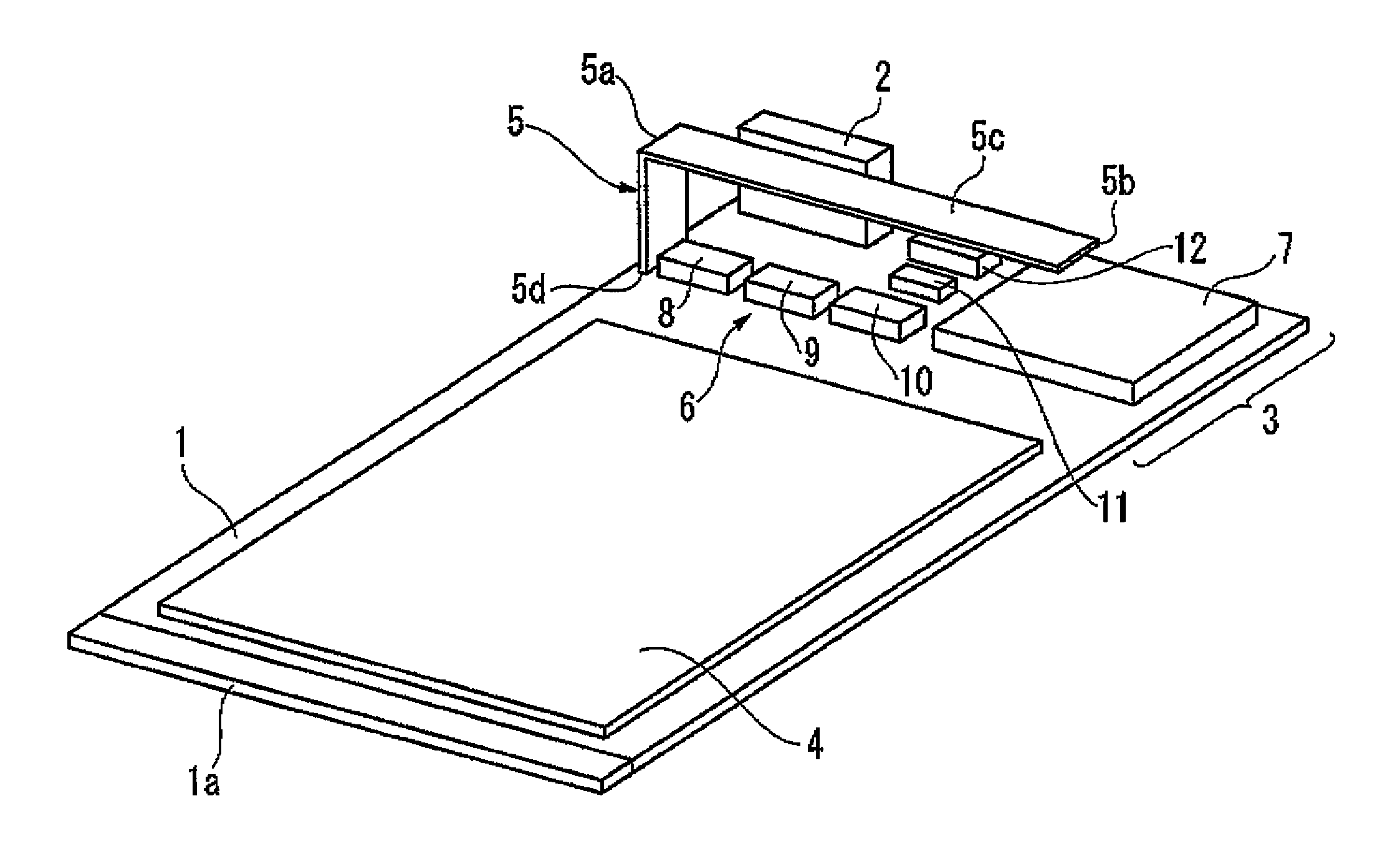
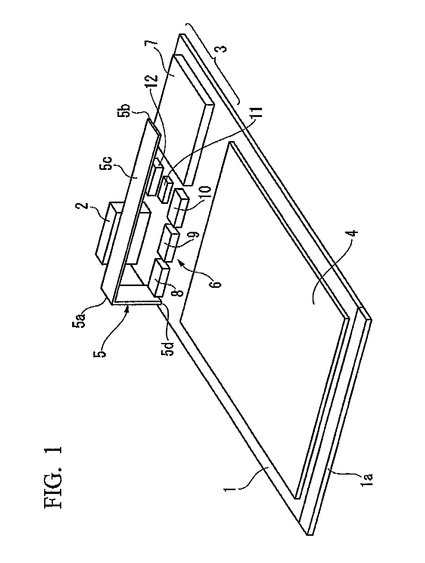
[0066]Hereinafter, in reference to FIGS. 1-6, one embodiment of a communication device of the present invention is explained. FIG. 1 is a perspective view of the outside of a communication device to which a solution for oscillation of the power amplifier is not applied. The communication device which is used while installed inside the case of a PC card includes: a printed wiring board 1; a chip antenna 2; an RF circuit portion 3; a digital circuit portion 4; and an L shape metallic plate 5 (conductive body). The RF circuit portion 3 has a constitution including a transmission portion 6 and a receiving portion 7, and the transmission portion 6 includes: an RFSAW filter 8; a power amplifier 9; an isolator 10; an RF switch 11; and a conductive body filter 12.

[0067]The printed wiring board 1 has a connector 1a at one end. The connector 1a is connected to a connector inside an extended slot of a notebook personal computer.

[0068]On the printed board 1, the chip antenna 2, the RF circuit p...

second embodiment

[0091]Hereinafter, in reference to FIGS. 7-9, a second embodiment of the present invention is explained. FIG. 7 is a perspective view of the outside of the communication device of this embodiment. The communication device which is used in a state of being installed inside a case of a PC card includes: a printed wiring board 21; a chip antenna 22; an RF circuit portion 23; a digital circuit portion 24; and an L shape metallic plate 25 (conductive body).

[0092]The printed wiring board 21 has a connector 21a at one end. The connector 21a is connected to a connector inside an extended slot of a notebook personal computer.

[0093]On the printed board 21, the chip antenna 22, the RF circuit portion 23 and the digital circuit portion 24 are provided in this order from a side of an end opposite to the connector 21a. In addition, the printed wiring board 21 has a ground conductive body to which the L shape metallic plate 25 is connected.

[0094]The chip antenna 22 is implemented so as to have a l...


PUM


Abstract

A communication device which solves a new problem, that is, a power amplifier has oscillation caused by providing a conductive body which reduces the effects of the noise on a chip antenna, includes: a chip antenna which catches radio waves of a desired frequency; an RF circuit which is implemented on a printed wiring board and which converts received signals input from the chip antenna to a low frequency; a digital circuit which is implemented on the printed wiring board and which demodulates the received signals in a low frequency input from the RF circuit; a conductive body which is extended between the chip antenna and the digital circuit while being maintained at a certain height from the printed wiring board, and which has an end connected to a ground conductive body of the printed wiring board; and a radio wave absorption body which is attached to the conductive body.

Description

CROSS-REFERENCE TO RELATED APPLICATIONS[0001]This application is a national stage of international application No. PCT / JP2007 / 056641, filed on Mar. 28, 2007, and claims the benefit of priority under 35 USC 119 of Japanese Patent Application No. 2006-087466 and 2006-087467, both filed on Mar. 28, 2006, which are incorporated herein by reference.TECHNICAL FIELD[0002]1. Field of the Invention[0003]The present invention relates to a communication device.[0004]2. Background Art[0005]In both the past and the present, there are various types of communication devices for wireless communication to external apparatuses such as a base station, for example, there is a type of PC card which is used after insertion into an extended slot of a mobile terminal or a notebook type personal computer (hereinafter, a notebook personal computer).[0006]Such a communication device provides an antenna for establishing a wireless communication to such a base station in order to transmit and receive radio wave...

Claims


Application Information

Patent Timeline
Patent Type & Authority Patents(United States)
IPC IPC(8): H01Q1/24
CPCH01Q1/243H01Q1/526H01Q17/00
Inventor KAWATA, TOSHIHIKONAKADA, SHINICHINOJI, MASAKI
Owner KYOCERA CORP
Why Eureka
Try Eureka