
Method to fabricate high performance carbon nanotube transistor integrated circuits by three-dimensional integration technology

a technology of integrated circuits and carbon nanotubes, applied in the field of carbon nanotube technology, can solve the problems of incompatibility of carbon nanotube growth, process limitation, and circuits involving carbon

Active Publication Date: 2013-06-04
GLOBALFOUNDRIES US INC
View PDF18 Cites 10 Cited by
  • Summary
  • Abstract
  • Description
  • Claims
  • Application Information

AI Technical Summary

Benefits of technology

The present invention provides techniques for fabricating carbon nanotube-based devices. One aspect of the invention is a method for fabricating a carbon nanotube-based integrated circuit by connecting carbon nanotubes with device elements on two wafers. Another aspect is a carbon nanotube-based integrated circuit that includes a first wafer with carbon nanotubes and a second wafer with device elements, where the first wafer is bonded to the second wafer to connect the carbon nanotubes with the device elements. The invention allows for the fabrication of highly integrated carbon nanotube-based devices, which can be useful in various fields such as electronics and sensors.

Problems solved by technology

One of the major challenges in utilizing devices and complex circuits involving carbon nanotubes lies in the incompatibility of the carbon nanotube growth conditions and the process limitation of current complementary metal-oxide-semiconductor (CMOS) technology.
However, during the subsequent processing, the deposited carbon nanotubes may be destroyed via oxidation and the properties of the carbon nanotubes may also be altered due to surface treatments.
Another practical challenge of realizing integrated circuits based on carbon nanotubes is the alignment of carbon nanotubes with the rest of the circuit components.
While there has been much progress in controlling the growth orientation and / or the deposition location of nanotubes, their alignment with the rest of the circuits has not been addressed.

Method used


Image

  • Method to fabricate high performance carbon nanotube transistor integrated circuits by three-dimensional integration technology
  • Method to fabricate high performance carbon nanotube transistor integrated circuits by three-dimensional integration technology
  • Method to fabricate high performance carbon nanotube transistor integrated circuits by three-dimensional integration technology

Examples


Embodiment Construction

[0025]In order to successfully use carbon nanotubes as active elements in a practical device and / or circuit, a new fabrication scheme is required to combine existing complementary metal-oxide-semiconductor (CMOS) technology and the carbon nanotubes. The present teachings provide such a fabrication scheme.

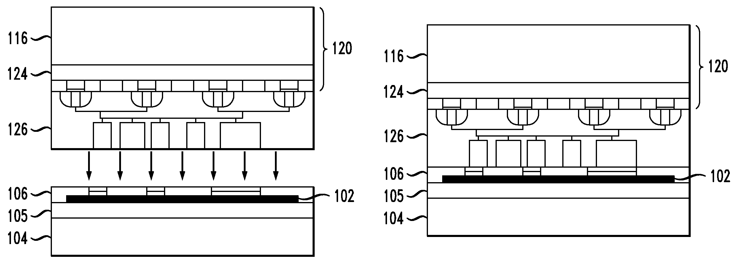
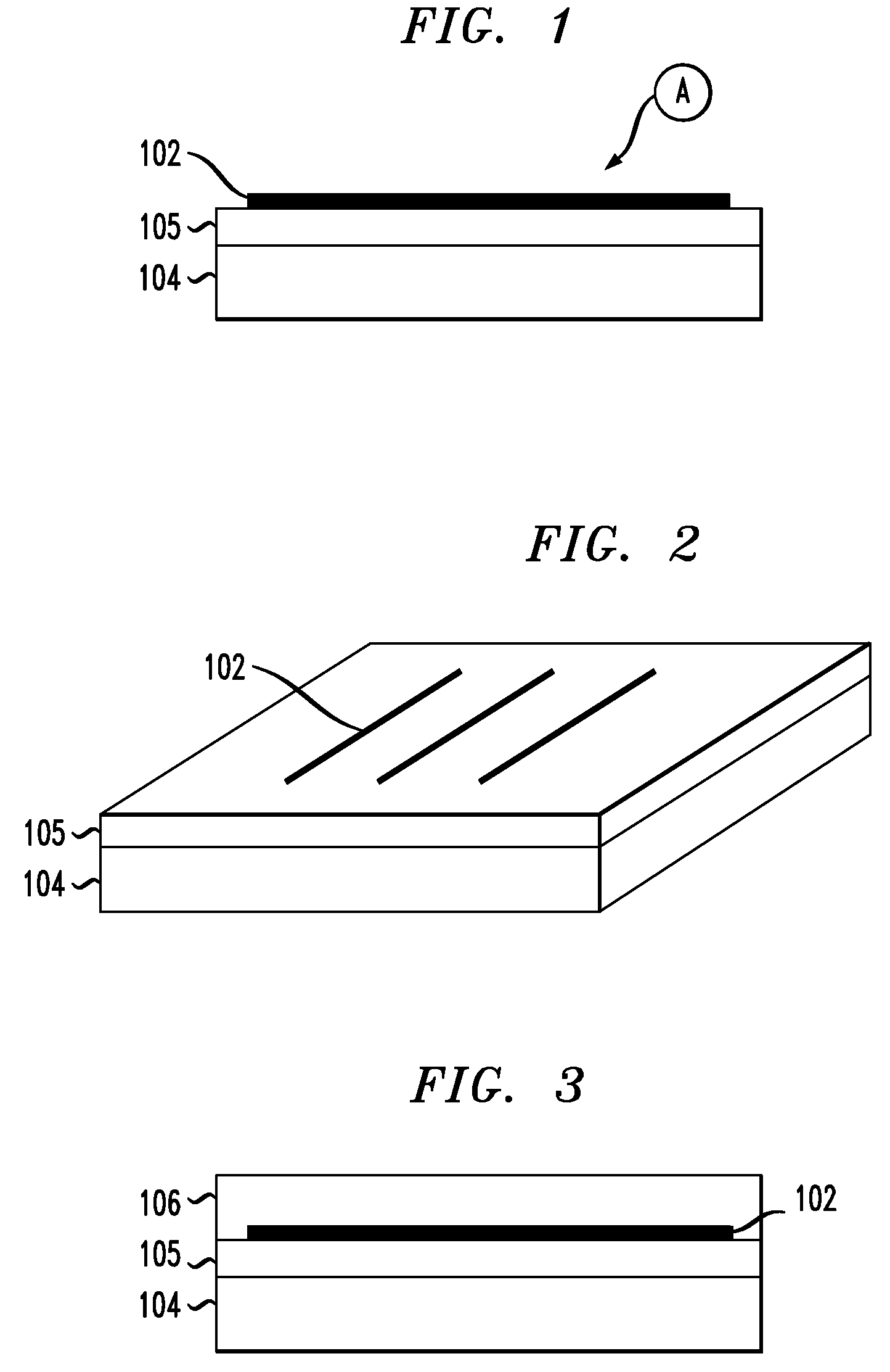
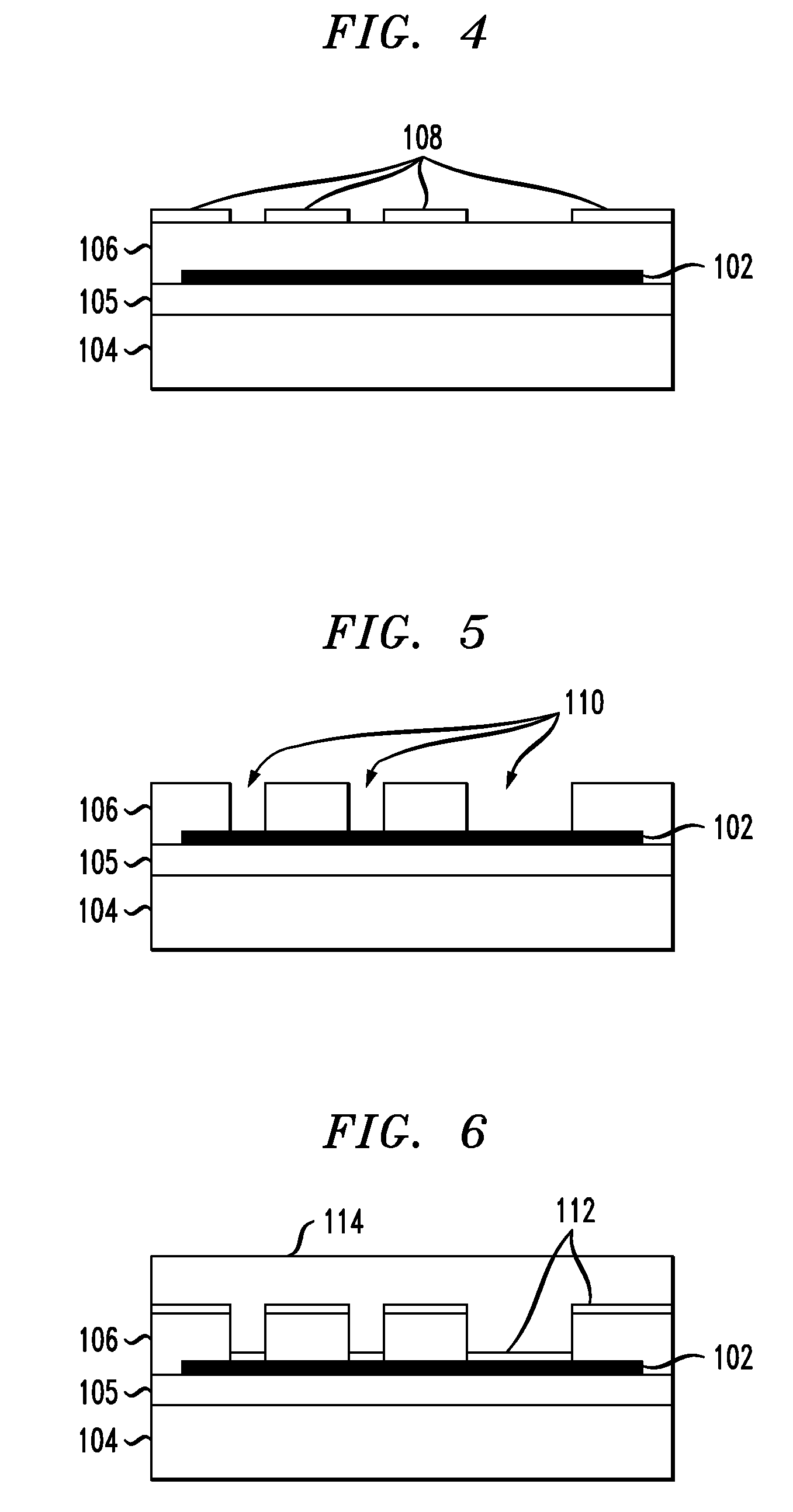
[0026]FIGS. 1-15 are diagrams illustrating an exemplary methodology for fabricating a carbon nanotube-based integrated circuit. In this particular example, carbon nanotube-based transistors are formed by providing carbon nanotubes fabricated on one substrate (referred to herein as a carbon nanotube wafer) and CMOS device elements (and associated wiring) on another substrate (referred to herein as a device wafer), then connecting the carbon nanotubes with one or more of the device elements through the use of face-to-face bonding to bond the carbon nanotube wafer and the device wafer together in a three-dimensional configuration.

[0027]Three-dimensional integration has become a very pr...


PUM

PropertyMeasurementUnit
thicknessaaaaaaaaaa
temperature capacityaaaaaaaaaa

Abstract

Techniques for fabricating carbon nanotube-based devices are provided. In one aspect, a method for fabricating a carbon nanotube-based integrated circuit is provided. The method comprises the following steps. A first wafer comprising carbon nanotubes is provided. A second wafer comprising one or more device elements is provided. One or more of the carbon nanotubes are connected with one or more of the device elements by bonding the first wafer and the second wafer together. A carbon nanotube-based integrated circuit is also provided.

Description

FIELD OF THE INVENTION[0001]The present invention relates to carbon nanotube technology and more particularly, to techniques for fabricating carbon nanotube-based devices.BACKGROUND OF THE INVENTION[0002]Carbon nanotubes possess extraordinary electronic properties that are attractive for high-speed and high-performance circuits. One of the major challenges in utilizing devices and complex circuits involving carbon nanotubes lies in the incompatibility of the carbon nanotube growth conditions and the process limitation of current complementary metal-oxide-semiconductor (CMOS) technology. For example, chemical vapor deposition (CVD) grown carbon nanotubes require a growth condition of at least 600° C. for producing high quality nanotubes, which exceeds the temperature capacity of about 350° C. to about 400° C. for CMOS processes.[0003]One possible solution to work around this temperature limitation is to deposit pre-formed carbon nanotubes on the substrate from a solution. However, du...

Claims


Application Information

Patent Timeline
Patent Type & Authority Patents(United States)
IPC IPC(8): H01L51/40
CPCB82Y10/00B82Y40/00H01L21/6835H01L21/76885H01L21/50H01L21/768H01L23/4827H01L2221/1094H01L2221/68359H01L2224/83894H01L2924/01025H01L2924/01029H01L2924/01046
Inventor AVOURIS, PHAEDONCHEN, KUAN-NENGLIN, YU-MING
Owner GLOBALFOUNDRIES US INC
Learn More