Semiconductor device
a technology of semiconductors and devices, applied in the direction of semiconductor devices, electrical equipment, transistors, etc., to achieve good electrical characteristics
- Summary
- Abstract
- Description
- Claims
- Application Information
AI Technical Summary
Benefits of technology
Problems solved by technology
Method used
Image
Examples
embodiment 1
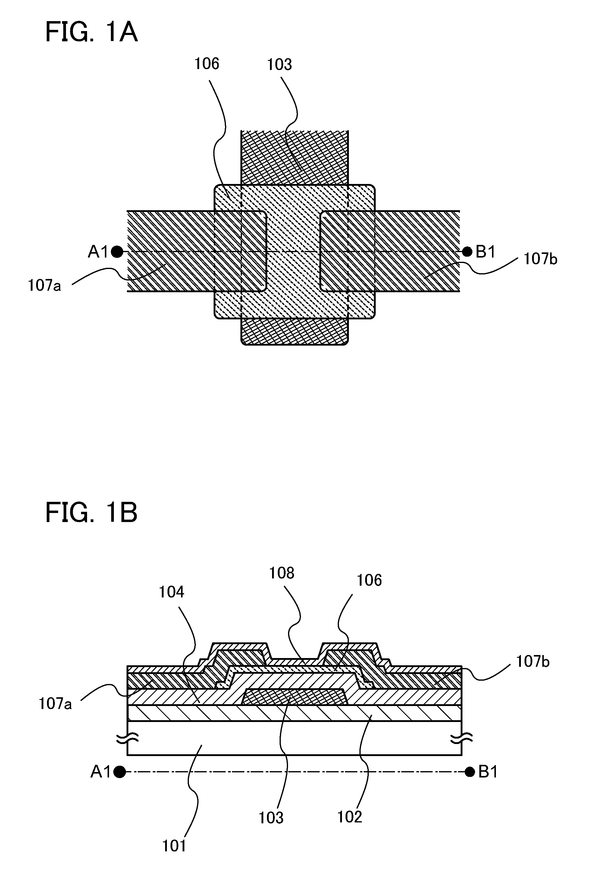
[0042]In this embodiment, a semiconductor device which is one embodiment of the present invention is described with reference to FIGS. 1A and 1B. Note that while a transistor is illustrated as an example of the semiconductor device in FIGS. 1A and 1B, one embodiment of the present invention can be similarly implemented using a diode and the like.
[0043]FIG. 1A is a top view of a transistor. FIG. 1B is a cross sectional view taken along line A1-B1 in FIG. 1A. The transistor includes, over a substrate 101, a base insulating layer 102, a gate electrode layer 103, a gate insulating layer 104, an oxide semiconductor layer 106 where a channel region is formed, a source electrode layer 107a and a drain electrode layer 107b, and an insulating layer 108 which covers the oxide semiconductor layer 106, the source electrode layer 107a, and the drain electrode layer 107b.
[0044]The transistor in FIGS. 1A and 1B is a transistor having a bottom-gate structure, in which the oxide semiconductor layer...
embodiment 2
[0124]In this embodiment, an example where a silicon oxide layer with a low hydrogen concentration is used as a base insulating layer of a top-gate transistor will be described with reference to FIGS. 7A to 7C. The silicon oxide layer is formed by a plasma CVD method using silicon tetrafluoride which is a deposition gas, nitrous oxide which is an oxidizing gas, and argon which stably generates plasma.
[0125]A base insulating layer 202 including silicon oxide as its main component is formed over the substrate 201. As described above, the base insulating layer 202 is formed by a plasma CVD method using silicon tetrafluoride. For details of the formation method, a manufacturing method of the gate insulating layer 104 in Embodiment 1 may be referred to. The thickness of the base insulating layer 202 is preferably five or more times as thick as the total thickness of an oxide semiconductor layer and a gate insulating layer which are formed later.
[0126]When the base insulating layer 202 ha...
embodiment 3
[0140]In this embodiment, an example where a silicon oxide layer with a low hydrogen concentration which is formed by using silicon tetrafluoride as a deposition gas is used as a base insulating layer of a top-gate transistor will be described with reference to FIGS. 8A to 8D.
[0141]A base insulating layer 302 including silicon oxide as its main component is formed over the substrate 301. As described above, the base insulating layer 302 is formed by a plasma CVD method using silicon tetrafluoride. For details of the formation method, a manufacturing method of the gate insulating layer 104 in Embodiment 1 may be referred to. The thickness of the base insulating layer 302 is preferably five or more times as thick as the total thickness of an oxide semiconductor layer and a gate insulating layer which are formed later.
[0142]After that, an In—Ga—Zn—O-based film with a thickness of 10 nm to 30 nm is formed by a sputtering method as an oxide semiconductor film 303. Then, a conductive film...
PUM
 Abstract
Description
Claims
Application Information
 - R&D
- Intellectual Property
- Life Sciences
- Materials
- Tech Scout
- Unparalleled Data Quality
- Higher Quality Content
- 60% Fewer Hallucinations
Browse by: Latest US Patents, China's latest patents, Technical Efficacy Thesaurus, Application Domain, Technology Topic, Popular Technical Reports.
© 2025 PatSnap. All rights reserved.Legal|Privacy policy|Modern Slavery Act Transparency Statement|Sitemap|About US| Contact US: help@patsnap.com


