
Power semiconductor device having adjustable output capacitance

a technology of output capacitance and output capacitance, which is applied in the direction of semiconductor devices, diodes, electrical apparatuses, etc., can solve the problems of increased device output capacitance, increased power loss, and extra electronic devices generating extra circuit costs, so as to reduce the cost of the power semiconductor device in the present invention and increase the output capacitance of the power semiconductor device.

Inactive Publication Date: 2013-01-29
ANPEC ELECTRONICS CORPORATION
View PDF2 Cites 5 Cited by
  • Summary
  • Abstract
  • Description
  • Claims
  • Application Information

AI Technical Summary

Benefits of technology

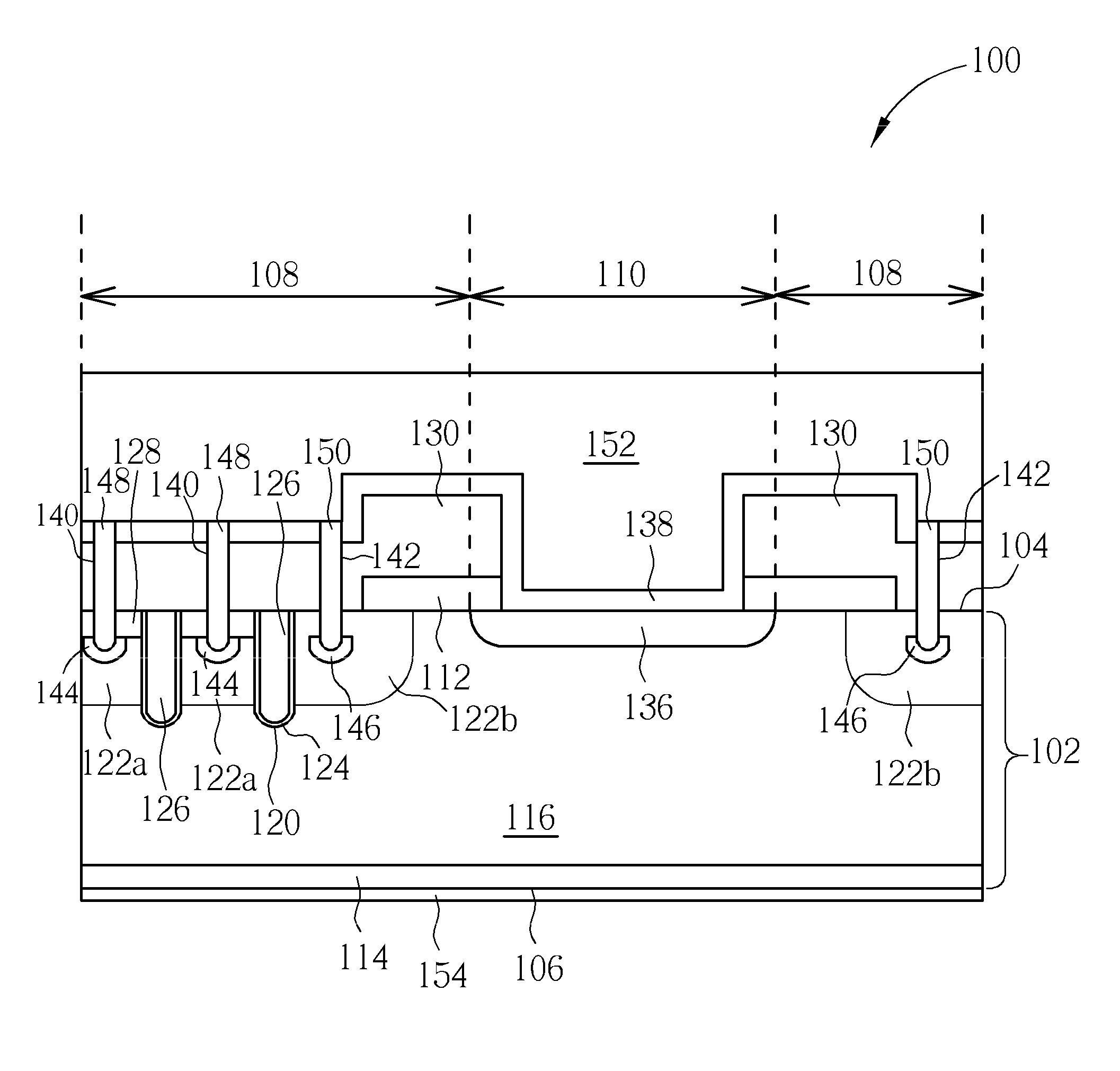
[0013]In the present invention, the manufacturing method of the power semiconductor device simultaneously fabricates the snubber capacitor in the step of fabricating the power transistor device, so that the power transistor device and the snubber capacitor are manufactured within a same power semiconductor device. The snubber capacitor and the power transistor device in the power semiconductor device use a same drain metal layer and a same source metal layer, and the snubber capacitor is electrically connected between the drain and the source of the power transistor device. Accordingly, the output capacitance of the power semiconductor device can be raised, and the problem of the voltage spikes is solved when the power semiconductor device is turned off. Further, the power semiconductor device in the present invention does not require electrically connecting to any extra snubber circuit, and the cost of the power semiconductor device in the present invention can be reduced.

Problems solved by technology

Therefore, the voltage spikes caused by turning off the conventional trench MOSFET device are increased, and higher power loss is generated.
However, the extra electronic device generates extra circuit cost, and increases extra manufacturing process of welding.
Thus the manufacturing cost is increased.

Method used


Image

  • Power semiconductor device having adjustable output capacitance
  • Power semiconductor device having adjustable output capacitance
  • Power semiconductor device having adjustable output capacitance

Examples


Embodiment Construction

[0023]Please refer to FIG. 3 through FIG. 10, which are schematic diagrams illustrating a manufacturing method of a power semiconductor device having an adjustable output capacitance according to a first embodiment of the present invention. First, as shown in FIG. 3, a semiconductor substrate 102 is provided. The semiconductor substrate 102 has a top surface 104 and a bottom surface 106, and the top surface 104 of the semiconductor substrate 102 has a first device region 108 and a second device region 110 defined thereon. The first device region 108 is defined to manufacture a power semiconductor device, and the second device region 110 is defined to manufacture a snubber capacitor. Then, the semiconductor substrate 102 in the second device region 110 is covered with a field oxide layer 112, and the semiconductor substrate 102 in the first device region 108 is exposed. Thus the semiconductor substrate 102 in the second device region 110 can be prevented from being affected by the fo...


PUM


Abstract

A power semiconductor device having adjustable output capacitance includes a semiconductor substrate having a first device region and a second device region defined thereon, at lest one power transistor device disposed in the first device region, a heavily doped region disposed in the semiconductor substrate of the second device region, a capacitor dielectric layer disposed on the heavily doped region, a source metal layer disposed on a top surface of the semiconductor substrate and electrically connected to the power transistor device, and a drain metal layer disposed on a bottom surface of the semiconductor substrate. The source metal layer in the second device, the capacitor dielectric layer and the heavily doped region form a snubber capacitor.

Description

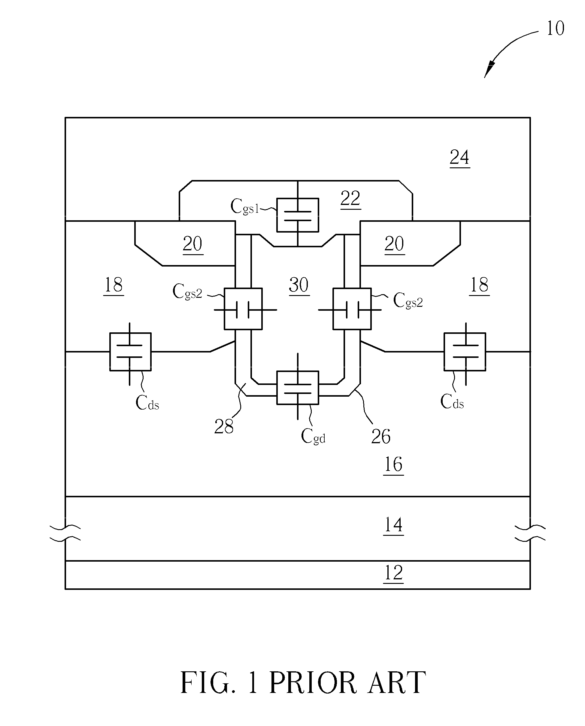
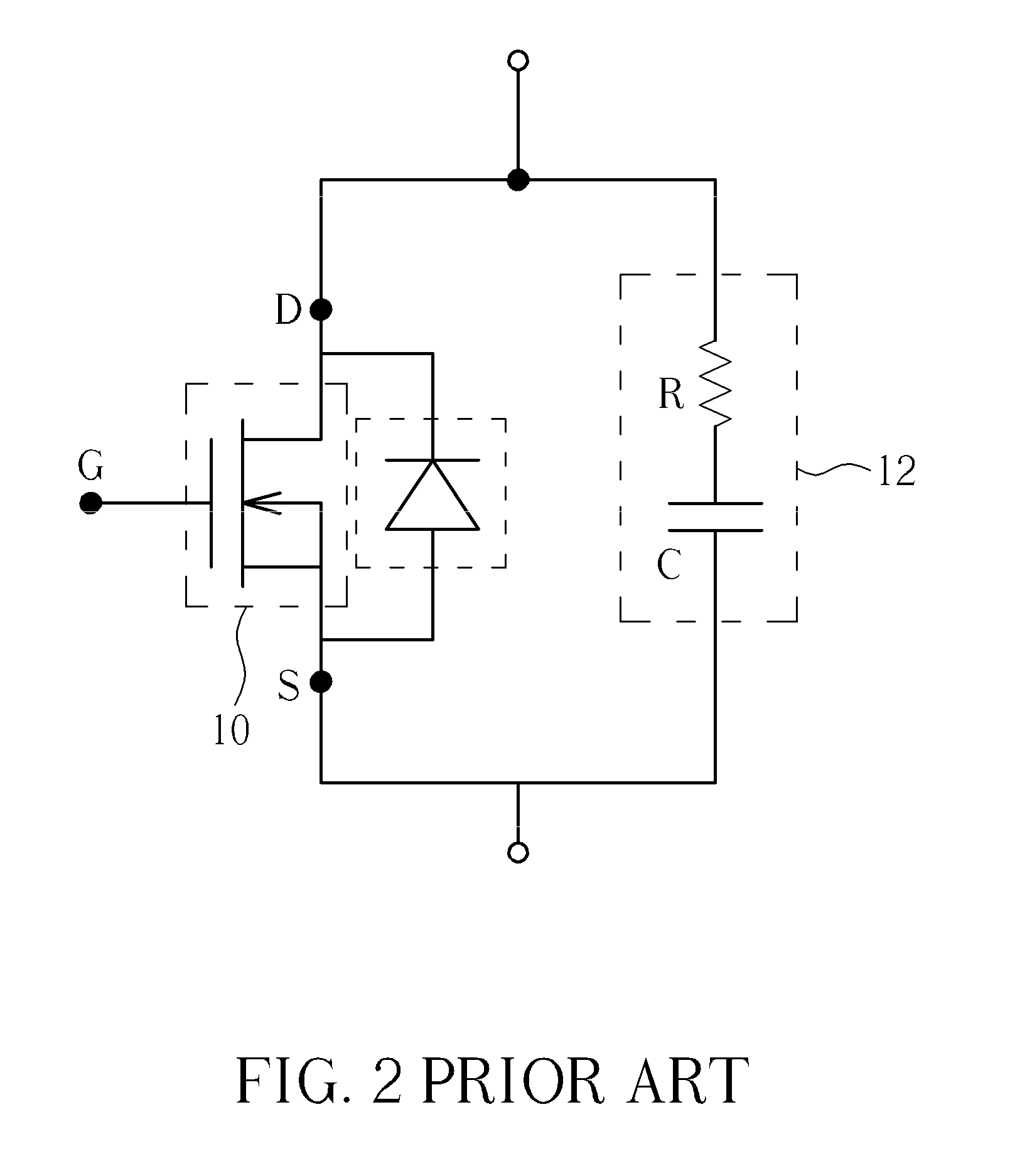
BACKGROUND OF THE INVENTION[0001]1. Field of the Invention[0002]The present invention relates to a power semiconductor device and a manufacturing method thereof, and more particularly to a power semiconductor device having adjustable output capacitance and a manufacturing method thereof.[0003]2. Description of the Prior Art[0004]Power semiconductor devices are typical semiconductor devices in power management applications, such as a switching power supply, a power control IC of a computer system or peripherals, a power supply of a backlight, motor controller, etc. Power semiconductor devices can include various kinds of transistors, such as an insulated gate bipolar transistor (IGBT) and a metal-oxide-semiconductor field effect transistor (MOSFET).[0005]Please refer to FIG. 1, which is a schematic diagram illustrating a cross-sectional view of a trench MOSFET device according to the prior art. As shown in FIG. 1, the conventional trench MOSFET device 10 of the prior art includes a d...

Claims


Application Information

Patent Timeline
Patent Type & Authority Patents(United States)
IPC IPC(8): H01L29/76
CPCH01L29/739H01L27/06H01L29/7813H01L27/0629H01L29/7803H01L29/41766H01L29/1095H01L29/66734H01L29/7806H01L29/0878H01L29/42368
Inventor LIN, WEI-CHIEHYANG, GUO-LIANGLIAO, SHIAN-HAU
Owner ANPEC ELECTRONICS CORPORATION
Learn More